VLSI Physical Design Essentials
Introduction to VLSI Physical Design
From Logic to Layout
Think of an integrated circuit, or a chip, as a bustling city. Before anyone lays a single brick, an architect creates a blueprint. This blueprint doesn't just show the buildings; it details the roads, the plumbing, the electrical grid, and how everything connects to ensure the city functions efficiently. VLSI physical design is the architectural phase for computer chips.
It's the process of transforming a circuit's logical plan, called a netlist, into a detailed physical layout that can be manufactured on a silicon chip.
This isn't just a simple conversion. The decisions made during physical design directly control the final chip's success. Every choice is a balancing act between three critical, often competing, factors known as PPA:
- Performance: How fast can the chip operate? This is determined by how quickly signals can travel between different components.
- Power: How much energy does the chip consume? A chip that gets too hot or drains a battery too quickly is not a good design.
- Area: How much silicon real estate does the chip occupy? Smaller chips are cheaper to manufacture, meaning more can be fit onto a single silicon wafer.
The Design Flow
To manage the staggering complexity of designing a chip with billions of transistors, engineers follow a structured sequence of steps called the physical design flow. Each stage builds upon the last, progressively refining the layout from a rough sketch into a final, manufacturable blueprint.
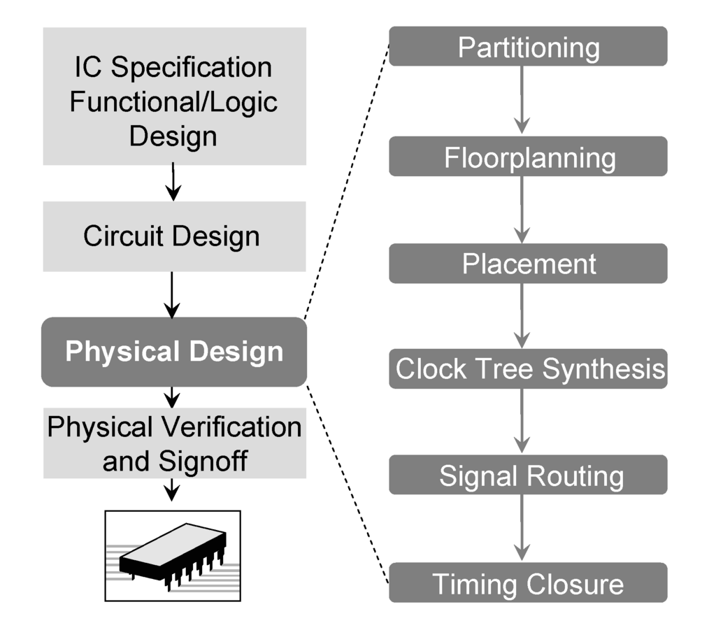
While the details are complex, the main stages are conceptually straightforward. Let's walk through the key steps shown in the diagram.
Key Stages of the Flow
Floorplanning is the first step. It’s like creating a zoning map for our chip city. Here, engineers decide the chip's overall shape and size. They allocate space for major functional blocks (like the CPU core, memory, and graphics unit) and plan the main pathways for power and data signals. Good floorplanning is crucial for avoiding traffic jams and ensuring all parts of the chip get the power they need.
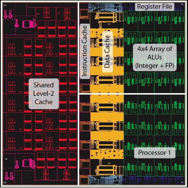
Placement comes next. With the major blocks in position, this stage involves precisely placing the millions of smaller, standard logic cells (like AND and OR gates) within their designated areas. The goal is to place cells that communicate frequently close to each other to minimize the length of the wires that will eventually connect them. Shorter wires mean faster signals and lower power consumption.
Routing is the process of connecting everything. Think of it as paving the roads and laying all the wiring in our city. Automated tools draw millions of tiny metal wires, or interconnects, to connect all the pins on all the cells according to the original logical netlist. This is done across multiple layers of metal, like a multi-level highway system, to ensure everything connects without creating short circuits.
Finally, Verification ensures the design is correct and manufacturable. Engineers run a battery of checks. Does the physical layout match the original logical design? Are there any short circuits or open connections? Does the design violate any of the complex rules set by the manufacturing facility? This final signoff confirms that the blueprint is ready to be sent for fabrication.
These stages work together to translate an abstract idea into a tangible, high-performance piece of technology. Now, let's test your understanding of these fundamental concepts.
In VLSI physical design, what are the three critical, often competing, factors represented by the acronym PPA?
Which stage of the physical design flow is most analogous to creating a city's zoning map, deciding where the residential, commercial, and industrial zones will be?