VLSI Design RTL to GDS
Introduction to VLSI Design
From Idea to Silicon
Nearly every piece of modern technology, from your smartphone to the servers that power the internet, runs on integrated circuits, or chips. Very Large Scale Integration (VLSI) is the science and art of packing millions, or even billions, of microscopic switches called transistors onto a single one of these chips. This incredible density is what gives our devices their power and speed.
But how do you design something so complex? You can't just start drawing transistors one by one. The process requires a highly structured workflow to turn an abstract idea into a physical, manufacturable product. This journey starts with a high-level description of what the chip should do and ends with a detailed geometric blueprint for manufacturing.
Two Languages of Design
At its core, digital design is about manipulating information represented by 1s and 0s. These binary values correspond to the on and off states of transistors. To manage this complexity, engineers use different levels of abstraction, much like a writer uses an outline before drafting a novel.
The design process begins at the Register-Transfer Level (RTL). This is a way of describing the chip's behavior, not its physical structure. An RTL description, typically written in a hardware description language (HDL) like Verilog or VHDL, specifies how data moves between registers (temporary storage units) and what logical operations are performed on that data. It's the functional blueprint, defining what the circuit must accomplish.
Think of RTL as an architect's plan. It shows which rooms connect and what each room is for, but it doesn't specify the brand of drywall or the type of nails to use.
The final destination is a file format called Geometric Data Stream (GDS), often shortened to GDSII. This file contains the complete physical layout of the chip. It's a massive collection of geometric shapes, polygons, and layers that tells the manufacturing facility exactly how to etch the transistors and wires onto a silicon wafer. It's the detailed construction manual, defining how the circuit is physically built.
The VLSI Design Flow
Getting from the abstract RTL description to the concrete GDS layout involves a series of automated steps known as the VLSI design flow. This process methodically translates the functional requirements into a physical reality, with checks and balances along the way.
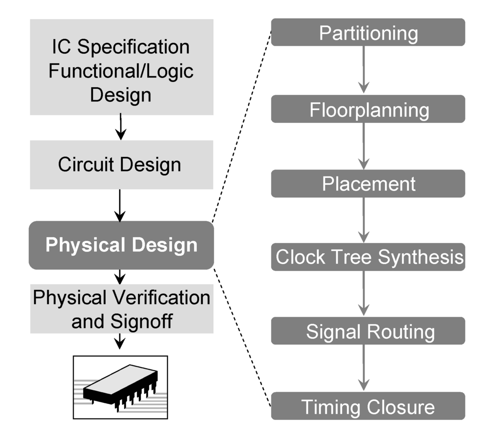
The journey can be broken down into a few key phases:
-
Logic Design: This is where the RTL is written. The designer creates a behavioral model of the chip, focusing entirely on functionality.
-
Logic Synthesis: An automated tool takes the RTL code and converts it into a list of fundamental digital components called logic gates (like AND, OR, and NOT gates). This step bridges the gap from behavior to a preliminary structure.
-
Physical Design: This is the most complex phase, where the list of gates is transformed into a physical layout. It involves several sub-steps:
- Floorplanning: Arranging the major functional blocks of the chip, much like deciding the general location of rooms in a house.
- Placement: Determining the precise location for every single logic gate within those blocks.
- Clock Tree Synthesis: Designing a network to distribute the clock signal, which synchronizes all the chip's operations, with extreme precision.
- Routing: Connecting all the gates and blocks with millions of tiny metal "wires" across several layers.
-
Signoff and Verification: Throughout the process, rigorous checks are performed to ensure the design is logically correct, meets timing and power requirements, and follows manufacturing rules. The final GDS file is generated only after the design passes all these checks.
This structured flow allows engineers to manage immense complexity, transforming a simple description of behavior into a powerful, intricate silicon chip ready for fabrication.