Understanding P-N Junctions
Semiconductor Basics
The Middle Ground
Some materials, like copper, let electricity flow through them easily. We call them conductors. Their electrons are loosely held and can move freely. Other materials, like glass, hold onto their electrons tightly and don't let electricity pass. These are insulators.
Semiconductors are the fascinating materials that fall somewhere in between. They aren't great conductors, but they aren't perfect insulators either. This unique property is what makes all modern electronics possible.
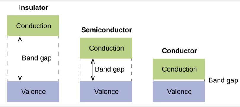
The key to this behavior lies in their atomic structure and something called an energy band gap. In any solid material, electrons occupy specific energy levels grouped into bands. The highest energy band filled with electrons is the valence band. The next band up, which is mostly empty, is the conduction band. For an electron to move and conduct electricity, it must jump from the valence band to the conduction band. The space between them is the band gap.
In conductors, the valence and conduction bands overlap, so electrons move with very little effort. In insulators, the band gap is huge, and it takes a massive amount of energy to get an electron to jump across. Semiconductors have a small, manageable band gap.
Pure and Simple
A perfectly pure semiconductor, with no impurities, is called an intrinsic semiconductor. Silicon is the most common example. In a crystal of pure silicon, each atom shares its four outer electrons with four neighbors, forming strong covalent bonds. All electrons are locked in place, holding the crystal together.
At absolute zero temperature, an intrinsic semiconductor acts like an insulator. No electrons are free to move. But if you add energy, perhaps by heating it, some electrons can gain enough energy to break free from their bonds and jump into the conduction band.
When an electron leaves its bond, it leaves behind an empty spot. This vacancy is called a hole, and it acts like a positive charge. A nearby electron can easily move into this hole, which makes the hole appear to move in the opposite direction. So, in an intrinsic semiconductor, we have two types of charge carriers: the negatively charged free electron and the positively charged moving hole.
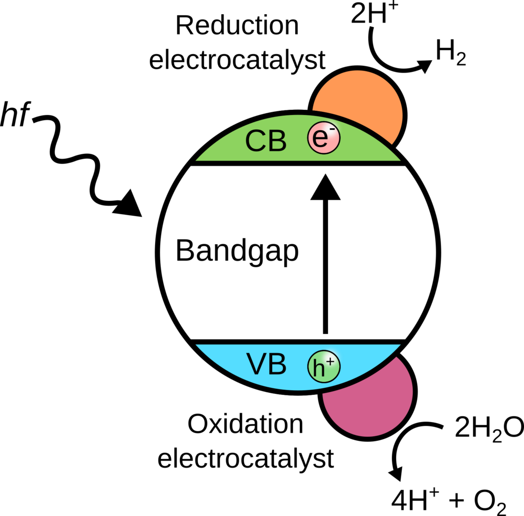
In an intrinsic semiconductor, the number of free electrons is always equal to the number of holes. However, there aren't very many of either, so pure semiconductors don't conduct electricity very well. To make them useful, we need to add a little something extra.
Adding Impurities
The real magic of semiconductors comes from a process called doping. Doping is the intentional introduction of tiny amounts of impurities into the semiconductor crystal. This process dramatically changes the material's electrical properties and creates an extrinsic semiconductor.
doping
noun
The process of intentionally introducing impurities into an intrinsic semiconductor to modulate its electrical properties.
There are two main types of doping.
To create an N-type semiconductor, we add an impurity that has more valence electrons than silicon. For example, phosphorus has five valence electrons. When a phosphorus atom replaces a silicon atom in the crystal, four of its electrons form bonds with the neighboring silicon atoms, but the fifth electron is left over. This extra electron is not part of any bond and is free to move around, becoming a charge carrier. Because the added carriers are negative electrons, the material is called N-type.
To create a P-type semiconductor, we do the opposite. We add an impurity with fewer valence electrons, like boron, which has three. When a boron atom replaces a silicon atom, it can only form three bonds. This leaves a hole where the fourth bond should be. This hole can readily accept an electron from a neighboring atom, causing the hole to move. Since the added carriers are positive holes, the material is called P-type.
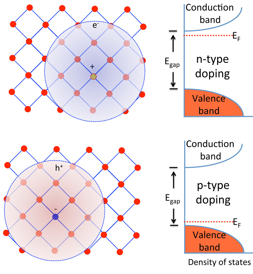
Through doping, we can precisely control the number and type of charge carriers in a semiconductor. In N-type material, electrons are the majority carriers and holes are the minority carriers. In P-type material, it's the reverse: holes are the majority carriers and electrons are the minority.
This ability to create materials with a surplus of either negative or positive charge carriers is the fundamental principle behind nearly all semiconductor devices, from diodes to transistors.
Let's check your understanding of these core concepts.
What is the key property of a semiconductor that distinguishes it from a conductor or an insulator?
In a pure, intrinsic semiconductor at room temperature, what are the charge carriers?
By combining these N-type and P-type materials, engineers can build the tiny switches and gates that power our digital world.