The Transistor Revolution
Semiconductor Basics
The Goldilocks Material
Some materials, like copper, let electricity flow freely. These are called conductors. Others, like rubber, block it completely. They're called insulators. But there's a third category of materials that are just right for building electronics: semiconductors.
Semiconductors, like silicon, can act as either a conductor or an insulator, depending on the conditions. This ability to switch between states is what makes them so useful. Think of it in terms of energy. For an electron to move and create a current, it needs to jump from its comfortable home orbit (the valence band) to a higher energy level where it can move freely (the conduction band). The gap between these two bands is called the band gap.
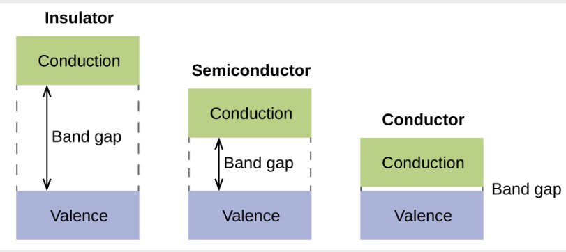
In a conductor, the bands overlap, so electrons can move with very little encouragement. In an insulator, the band gap is huge, and electrons are stuck. A semiconductor's band gap is small enough that we can give electrons a little push—with heat or an electric field—to get them moving.
Creating Charge Carriers
In a pure semiconductor, there aren't many free electrons to carry a current. To change that, we use a process called doping. This involves intentionally adding tiny amounts of impurities to the semiconductor crystal.
Imagine a silicon crystal where every atom is bonded to four neighbors. If we replace a silicon atom with an atom that has five outer electrons, like phosphorus, there will be one leftover electron. This electron is free to move around and carry a current. This is called an n-type semiconductor, because the charge carriers are negative electrons.
What if we add an atom with only three outer electrons, like boron? Now there's a missing bond, an empty spot where an electron should be. This empty spot is called a hole.
hole
noun
The absence of an electron in a semiconductor's crystal lattice. It acts as a positive charge carrier because a nearby electron can move into the hole, effectively causing the hole to move.
A hole behaves like a positive charge. When a neighboring electron moves into the hole, the hole effectively moves to the electron's previous location. It’s like a bubble rising in water—the bubble is just an absence of water, but it moves. This is a p-type semiconductor, because the charge carriers are positive holes.
The P-N Junction
Things get really interesting when we join a piece of p-type semiconductor with a piece of n-type semiconductor. This interface is called a p-n junction, and it's the fundamental building block of most semiconductor devices, including transistors.
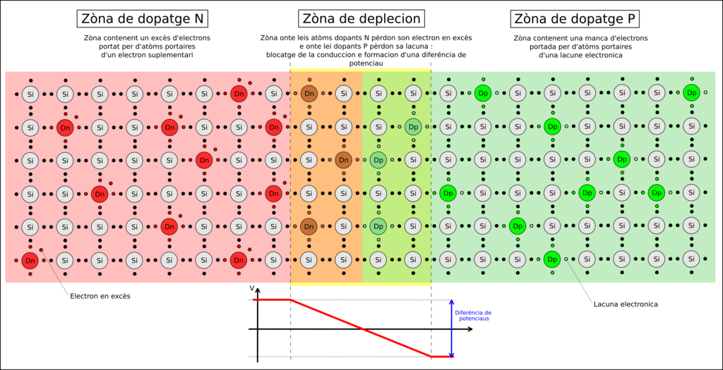
When the two materials first meet, the free electrons on the n-side see all the empty holes on the p-side and rush over to fill them. This process is called diffusion. As electrons move into holes, they neutralize each other, leaving behind a region near the junction that has no free charge carriers. This area is called the depletion region because it's depleted of mobile charges.
The movement of electrons leaves behind positively charged donor atoms on the n-side and creates negatively charged acceptor atoms on the p-side. This separation of charge creates a small electric field across the depletion region, pointing from the n-side to the p-side.
This electric field acts like a barrier. It pushes electrons away from the p-side and holes away from the n-side, preventing any more diffusion. The junction is now in equilibrium.
The p-n junction has a remarkable property: it allows current to flow easily in one direction but not the other. This one-way-gate behavior is what enables the control of electrical signals that is essential for all of modern electronics.
With this understanding of how semiconductors and p-n junctions work, we're ready to see how these simple structures can be combined to create a transistor.