The Semiconductor Industry Explained
Introduction to Semiconductors
What is a Semiconductor?
At the heart of every smartphone, computer, and modern car is a special class of material: the semiconductor. So what makes it so special?
Think of a material's ability to conduct electricity as a spectrum. On one end, you have conductors, like copper, which let electricity flow freely. On the other end are insulators, like rubber, which stop electricity in its tracks. Semiconductors sit right in the middle. They aren't great conductors, but they aren't perfect insulators either. Their name gives it away: semi-conducting.
Their key feature is that we can precisely control their conductivity. We can switch them from being more like an insulator to more like a conductor. This control is the foundation of all modern electronics. The most common semiconductor is silicon, the main component of sand.

To understand how this works, we need to look at electrons. In any material, electrons exist in energy levels, or bands. For an electron to move and create an electric current, it needs to jump from a lower energy band (the valence band) to a higher one (the conduction band). The space between these two is called the band gap.
In an insulator, this gap is huge, and electrons can't make the jump. In a conductor, the bands overlap, so electrons move freely. In a semiconductor, the gap is small enough that a little push—like adding energy in the form of heat or light—can get electrons to jump across.
Pure vs. Modified
A perfectly pure semiconductor, like a crystal of pure silicon, is called an intrinsic semiconductor. It doesn't conduct electricity very well on its own because its electrons are all locked into place, forming stable bonds with neighboring atoms. To make it useful, we need to introduce impurities.
This process of deliberately adding tiny amounts of other elements to a semiconductor is called doping. A doped semiconductor is known as an extrinsic semiconductor. Doping changes the material's electrical properties in a predictable way, giving us two main types.
doping
noun
The intentional introduction of impurities into an intrinsic semiconductor to modulate its electrical properties.
N-type Semiconductors
To make an n-type (negative-type) semiconductor, we dope silicon with an element that has one more electron in its outer shell, like phosphorus. When a phosphorus atom takes the place of a silicon atom in the crystal lattice, four of its outer electrons form bonds with the silicon neighbors. But that fifth electron is left over. It's not part of a bond, so it's free to move around. These free electrons act as charge carriers, allowing current to flow.
P-type Semiconductors
To create a p-type (positive-type) semiconductor, we do the opposite. We dope silicon with an element that has one fewer electron in its outer shell, like boron. When a boron atom replaces a silicon atom, it can only form three bonds. This leaves a gap where a fourth electron should be. This gap is called a hole. A nearby electron can jump into this hole, leaving a new hole behind. This movement of holes acts like a flow of positive charge.
In n-type material, the main charge carriers are negative electrons. In p-type material, the main charge carriers are positive holes.
The Heart of Electronics
Neither n-type nor p-type semiconductors are very exciting on their own. The magic happens when you join them together to form a p-n junction. This junction is the fundamental building block of most semiconductor devices, including diodes and transistors.
At the boundary where the p-type and n-type materials meet, the free electrons from the n-side diffuse over to fill the holes on the p-side. This creates a thin layer at the junction called the depletion region, which is empty of any free charge carriers and acts as an insulator.
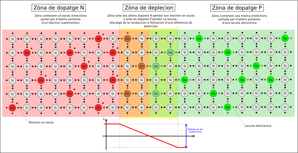
By applying an external voltage, we can control this depletion region. If we apply the voltage one way (forward bias), the region shrinks, allowing current to flow across the junction. If we apply it the other way (reverse bias), the region grows, blocking the current. This one-way-street behavior creates a diode, a component that lets electricity flow in only one direction.
By combining p-n junctions in specific ways, we can create transistors. A transistor can act as a tiny electronic switch, turning a current on or off, or as an amplifier, boosting a weak signal into a strong one. Billions of these microscopic transistors are etched onto a single silicon chip, working together to perform the complex calculations that power our digital world.
Let's review the key terms we've covered.
Ready to check your understanding?
How does a semiconductor's ability to conduct electricity compare to other materials?
The process of deliberately adding tiny amounts of impurities to a pure semiconductor to change its electrical properties is known as ______.
From this simple foundation of controlling electron flow, the entire field of modern electronics is built. Every task your phone or computer performs comes down to billions of semiconductor switches flipping on and off at incredible speeds.