The Journey of a Chip
Introduction to Semiconductors
The Material That Thinks
At the heart of every smartphone, computer, and digital device is a material with a curious property. It's not quite a conductor, which lets electricity flow freely like copper wire. And it's not an insulator, which blocks electricity completely like rubber. It's something in between.
semiconductor
noun
A material, typically a solid chemical element or compound, that can conduct electricity under some conditions but not others, making it a good medium for the control of electrical current.
This middle-ground ability is a semiconductor's superpower. Its conductivity isn't fixed. We can precisely control it, turning it from more of an insulator to more of a conductor on command. This control is the fundamental principle behind all modern electronics.
Silicon Valley's Star
Many materials can act as semiconductors, but one reigns supreme: silicon. There's a reason California's tech hub isn't called "Germanium Valley." Silicon is the second most abundant element in the Earth's crust, after oxygen. It's found in sand and quartz, making it incredibly cheap and accessible.
Pure silicon is a fairly poor conductor. To make it useful, it's modified through a process called doping. This involves intentionally introducing tiny amounts of impurities into the silicon crystal structure. Doping changes silicon's electrical properties in one of two ways:
- N-type: Adding an element like phosphorus, which has one more electron in its outer shell than silicon, creates a surplus of free-moving electrons. Since electrons have a negative charge, this is called N-type silicon.
- P-type: Adding an element like boron, which has one fewer electron, creates an electron deficit. This deficit is called a "hole," and it acts like a positive charge carrier. This is called P-type silicon.
By doping silicon, we can create materials with either an excess of negative charge carriers (electrons) or an excess of positive charge carriers (holes).
The On/Off Switch
The real magic happens when you press a piece of P-type silicon against a piece of N-type silicon. The boundary where they meet is called a P-N junction. At this junction, the excess electrons from the N-type side are drawn to the holes on the P-type side, creating a small region with no free charge carriers called the depletion region.
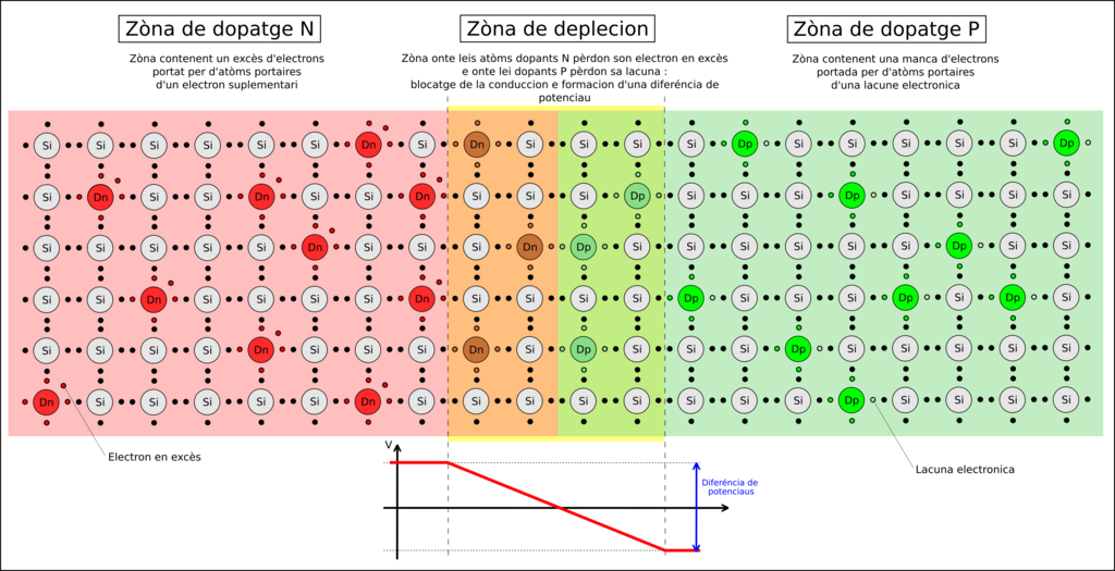
This depletion region acts like a one-way gate for electricity. Current can easily flow from the P-side to the N-side, but it's strongly resisted in the opposite direction. This simple P-N junction is the basis of a component called a diode.
But what if we sandwich them together, like N-P-N or P-N-P? This creates a transistor. A transistor is a tiny, semiconductor-based switch. A small electrical voltage applied to the middle layer can control a much larger current flowing through the other two layers. It can turn the current on or off completely.
The transistor is arguably the most important invention of the 20th century. It's the fundamental building block of all digital logic.
This simple on/off capability is everything. The "on" state can represent a 1, and the "off" state can represent a 0. By combining billions of these microscopic transistor switches on a single piece of silicon—an integrated circuit, or chip—we can perform complex calculations, store data, and run the software that powers our world.
What is the primary characteristic of a semiconductor material?
The process of intentionally adding impurities like phosphorus or boron to silicon is known as __________.
Everything from the processor in your laptop to the memory in your phone is built from these fundamental semiconductor principles.