Solar Photovoltaic Technology
Semiconductor Physics
The Structure of Silicon
At the heart of most solar panels is silicon, an element that makes up a huge portion of the Earth's crust. On its own, a single silicon atom has four electrons in its outer shell, called valence electrons. To become stable, it wants to have eight. So, in a solid crystal, each silicon atom shares one of its valence electrons with four of its neighbors. This forms a neat, repeating grid held together by strong covalent bonds.
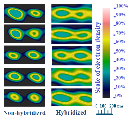
This crystalline structure is very stable. All the valence electrons are locked into these bonds, which means they aren't free to roam around. As a result, pure crystalline silicon is a poor conductor of electricity. To make it useful for electronics, we need a way to set some of those electrons free.
Energy Bands and the Bandgap
In an individual atom, electrons occupy distinct energy levels. But when billions of atoms are packed into a crystal, these levels merge into continuous energy bands. The outermost band filled with the bonded valence electrons is called the valence band. Above it lies the conduction band, an energy range where electrons are detached from their atoms and free to move, enabling electrical current.
For an electron to jump from the valence band to the conduction band, it needs to absorb enough energy to cross a forbidden zone separating them. This energy difference is called the energy. The size of the bandgap determines a material's electrical properties. Conductors have no bandgap, insulators have a very large one, and semiconductors like silicon have a small, useful bandgap.
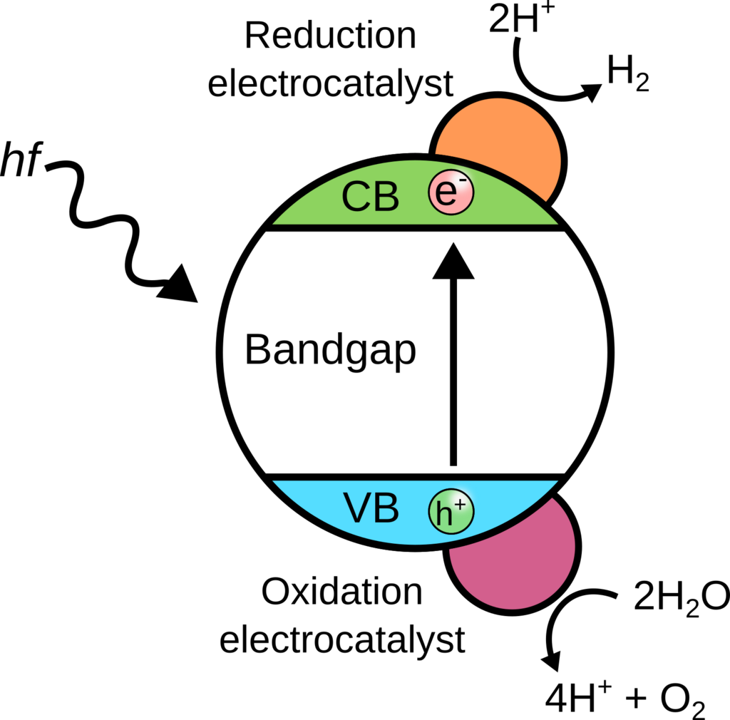
In a solar cell, photons from sunlight provide the energy for electrons to make this jump. When a photon with energy greater than the bandgap strikes the silicon, it excites an electron, elevating it into the conduction band. This process leaves behind a vacancy in the valence band called a hole. Both the free electron and the hole can then be guided to create an electric current.
Creating Charge Carriers with Doping
To improve silicon's conductivity and control the flow of charge, manufacturers intentionally introduce impurities into the crystal lattice. This process is called and it creates two distinct types of semiconductor material: N-type and P-type.
N-type (Negative) Silicon To create N-type material, silicon is doped with an element that has five valence electrons, like phosphorus. When a phosphorus atom replaces a silicon atom in the crystal, four of its valence electrons form bonds with the neighboring silicon atoms. The fifth electron is left over. It's not part of any bond and is only loosely held, so it requires very little energy to move into the conduction band and become a free charge carrier. Since electrons have a negative charge, this is called N-type silicon.
P-type (Positive) Silicon To create P-type material, the silicon is doped with an element that has only three valence electrons, such as boron. When a boron atom takes a silicon atom's place, it can only form bonds with three of its neighbors. This leaves a missing bond, creating a vacancy or "hole." This hole can easily accept an electron from a nearby bond. When an electron moves to fill the hole, it leaves a new hole behind. This movement of holes acts as the flow of positive charge. This is P-type silicon.
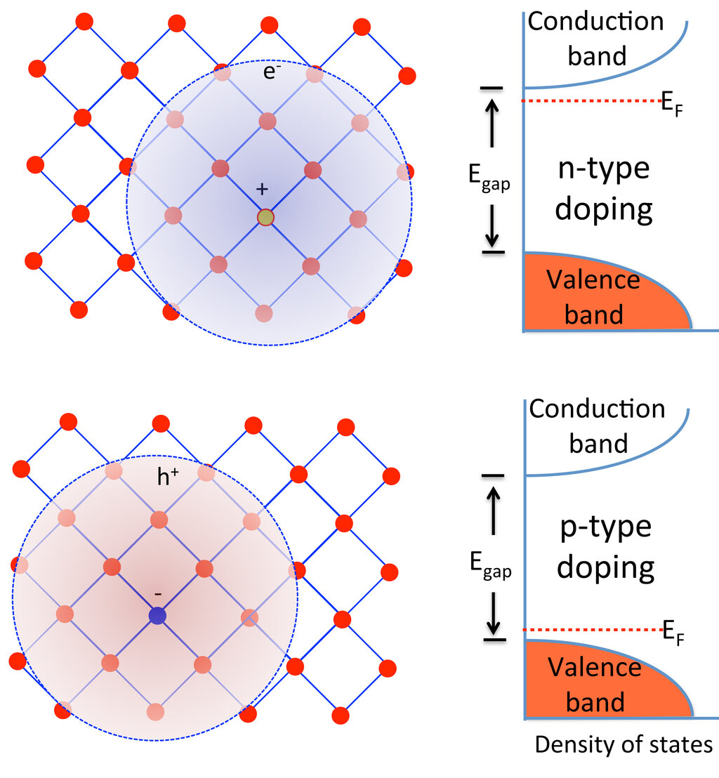
In N-type material, the vast majority of charge carriers are free electrons. We call them the majority carriers, while the few thermally generated holes are the minority carriers. The situation is reversed in P-type material, where holes are the majority carriers and electrons are the minority carriers. This distinction is the key to how a solar cell works, as we'll see when we combine these two materials to form a p-n junction.
By precisely controlling the doping process, engineers can fine-tune the electrical properties of silicon, turning a simple element into the foundation of complex photovoltaic systems.