Silicon Wafer Processing for Power Electronics
Introduction to Semiconductors
What Are Semiconductors?
Most materials either conduct electricity well, like copper, or block it completely, like rubber. Conductors let electrons flow freely, while insulators hold them tight. Semiconductors are the fascinating materials that fall somewhere in between. They can act as either a conductor or an insulator, depending on the conditions. This unique ability to control the flow of electricity is what makes them the foundation of all modern electronics.
Semiconductor
noun
A material with electrical conductivity between that of a conductor and an insulator.
While several materials have semiconductor properties, one element reigns supreme in the industry: silicon. Why silicon? It's the second most abundant element in the Earth's crust (after oxygen), making it inexpensive and readily available. More importantly, its atomic structure is perfectly suited for controlling electrical current.
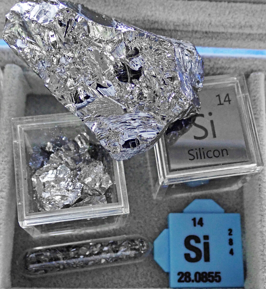
At its core, a silicon atom has four electrons in its outer shell, called valence electrons. In a pure silicon crystal, each atom shares these four electrons with its four neighbours, forming strong, stable bonds. This leaves no free electrons to move around and carry a current. In its pure state, silicon is actually a poor conductor of electricity, much like an insulator.
Making Silicon Conductive
To turn silicon into a useful semiconductor, its conductivity must be precisely manipulated. This is done through a process called doping. Doping involves intentionally introducing tiny amounts of impurities into the pure silicon crystal. These impurities are other elements that change silicon's electrical properties.
There are two main types of doping:
N-type Doping: An element with five valence electrons, like phosphorus, is added. Four of phosphorus's electrons bond with neighbouring silicon atoms, but the fifth is left over. This extra electron is free to move, increasing the material's conductivity. It's called N-type because the charge carriers are negative electrons.
P-type Doping: An element with three valence electrons, such as boron, is added. When boron bonds with four silicon neighbours, it's one electron short. This creates a vacant spot, or a "hole." A nearby electron can jump into this hole, leaving a new hole behind. This movement of holes acts like the flow of positive charge. It's called P-type for positive.
The true power of semiconductors is unlocked when a piece of P-type silicon is joined to a piece of N-type silicon. The boundary where they meet is called a P-N junction, and it's the fundamental building block of most semiconductor devices, including diodes and transistors.
The Heart of Electronics
At the P-N junction, the free electrons from the N-type side are attracted to the holes on the P-type side. They diffuse across the junction and combine. This creates a thin layer at the boundary, called the depletion region, which has no free charge carriers. This region acts as a barrier, preventing further current flow.
However, by applying an external voltage, we can control this barrier. Applying a voltage in one direction (forward bias) shrinks the depletion region, allowing current to flow easily. Applying it in the opposite direction (reverse bias) widens the barrier, blocking the current. This one-way-gate effect is the principle behind a diode.
Transistors, the switches that power our computers, take this a step further. A common type of transistor is like a sandwich of these materials, such as N-P-N. A small voltage applied to the middle 'P' layer can control a much larger current flowing through the two 'N' layers. This allows a tiny signal to switch a large current on or off, which is the basis of digital logic and amplification.
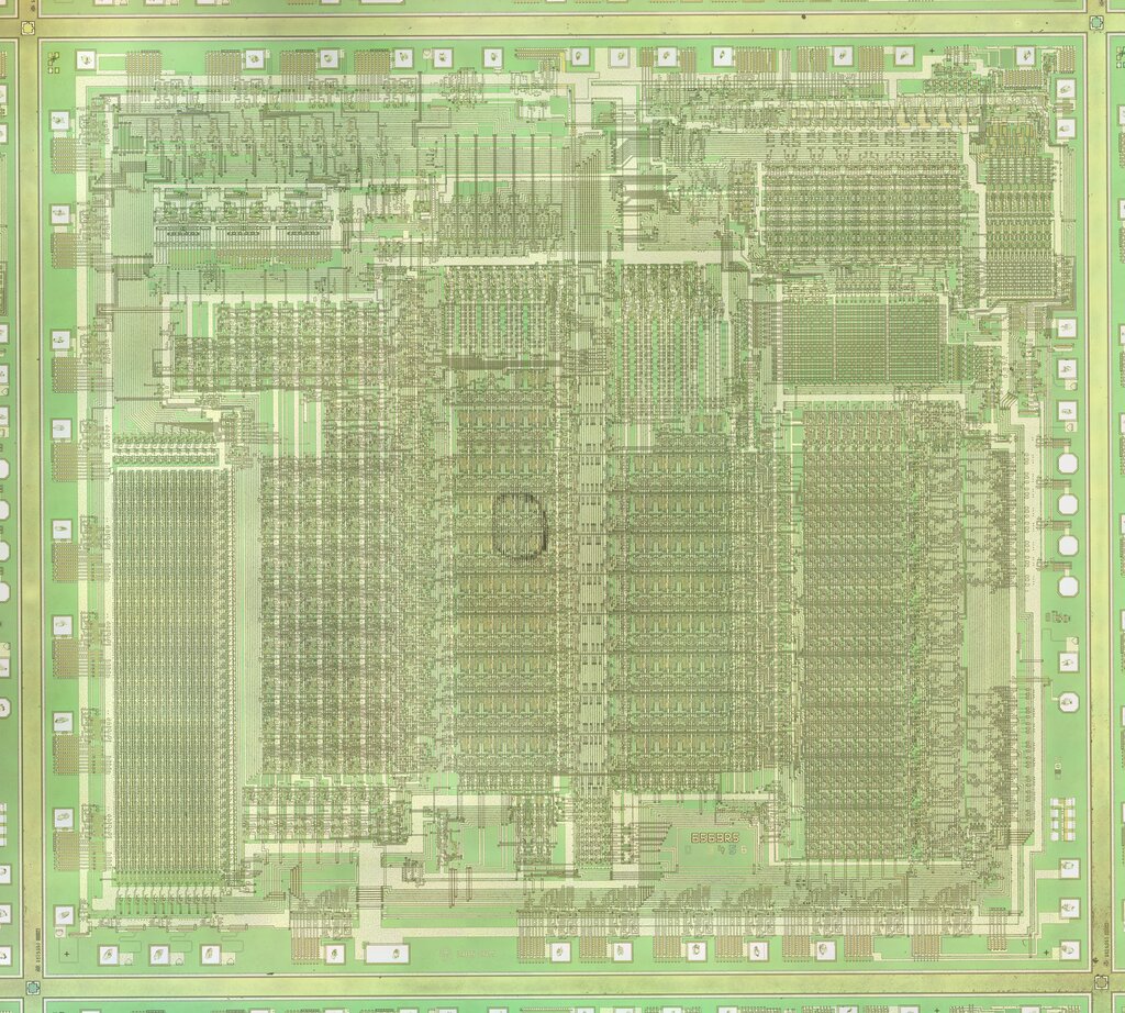
From simple diodes to complex microprocessors containing billions of transistors, these principles of controlling silicon's conductivity are fundamental. Understanding how semiconductors work is the first step to understanding how all modern power electronics operate.
Now, let's test your understanding of these fundamental concepts.
What is the primary characteristic of a semiconductor material?
Why is silicon the most commonly used material for semiconductors?
By doping silicon and creating P-N junctions, engineers can build the intricate components that power everything from your phone to the electrical grid.