Silicon Realization From Design to Production
VLSI Implementation Flow
From Code to Silicon
A modern chip design doesn't start with drawing transistors. It begins with code. Architects and designers describe the chip's behavior at a high level of abstraction, focusing on how data moves between registers and what operations are performed on it. This description is called Register Transfer Level, or RTL.
RTL
noun
Register Transfer Level. A design abstraction that models a digital circuit by specifying the flow of signals (data) between hardware registers and the logical operations performed on those signals.
Think of RTL as a blueprint for the chip's functionality, not its physical structure. Designers use a Hardware Description Language (HDL) like Verilog or VHDL to write the RTL. This code is descriptive, not prescriptive; it defines what the circuit should do, not how to build it with physical gates.
// Simple Verilog RTL for a 4-bit adder
module adder (
  input  [3:0] a,    // 4-bit input 'a'
  input  [3:0] b,    // 4-bit input 'b'
  output [3:0] sum   // 4-bit output 'sum'
);

  // Describe the behavior: sum is the result of a + b
  assign sum = a + b;

endmodule
Logic Synthesis
The RTL code is just a text file. To turn it into a circuit, we need a process called logic synthesis. This is where the magic happens. A synthesis tool, like Synopsys's Design Compiler or Cadence's Genus, takes the RTL as input and converts it into a gate-level netlist.
A gate-level netlist is a detailed map of the design, described as a connection of basic logic gates (like AND, OR, NOT) and flip-flops from a specific technology library.
The synthesis tool is incredibly sophisticated. It doesn't just do a direct translation. It optimizes the circuit based on a set of constraints you provide. This is where we first encounter the fundamental trade-off in chip design: Power, Performance, and Area (PPA).
| Metric | Goal | Trade-off Example |
|---|---|---|
| Power | Minimize consumption | Using slower, low-power gates might hurt performance. |
| Performance | Maximize clock speed | Faster gates are often larger and consume more power. |
| Area | Minimize silicon space | A smaller layout might create wiring congestion. |
During synthesis, the EDA tool tries to find the best possible combination of gates to meet your PPA targets. It might swap a large, fast gate for a smaller, slower one to save area, or add buffers to strengthen a signal and improve timing, at the cost of more power and area.
Physical Design
After synthesis, we have a logical blueprint (the netlist), but no physical one. The physical design stage takes this netlist and creates the actual geometric layout of the chip that will be sent for manufacturing. This entire process is often called the RTL-to-GDSII flow, where GDSII is the final file format that fabrication plants use.
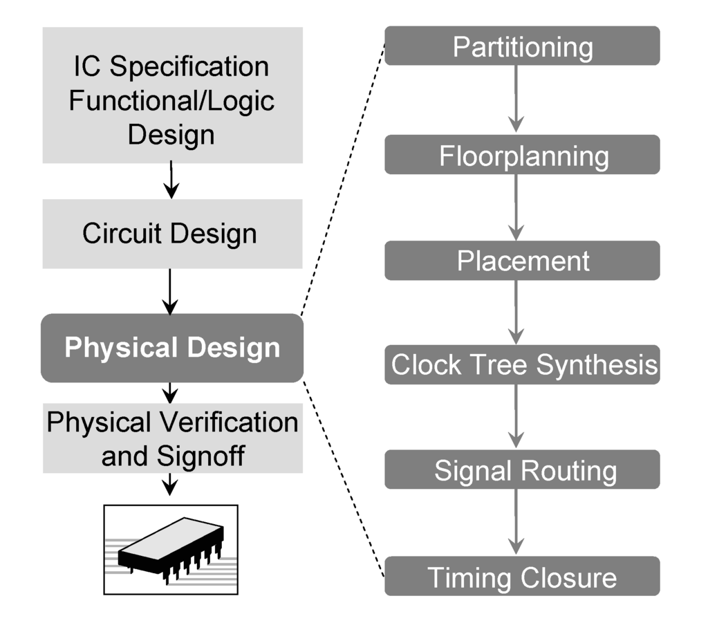
This process involves several critical steps, each managed by complex Electronic Design Automation (EDA) tools.
Physical Design (PD) in VLSI is one of the most critical stages in converting a logical circuit into a real, manufacturable chip.
The first step is floorplanning. Here, the engineer defines the overall shape and size of the chip. Large pre-designed blocks, known as macros (like memory or CPU cores), are placed on the chip's virtual real estate. You also plan out the power grid that will deliver electricity to all the components.
Next comes placement. The EDA tool takes the millions or billions of standard cells from the netlist and finds a specific location for each one on the chip. A good placement algorithm is crucial. It tries to place cells that are connected to each other close together to minimize wire length, which improves performance and reduces power consumption. Poor placement can lead to thermal hotspots or areas so dense with cells that they become impossible to wire up later, a problem known as congestion.
After placing the cells, we must ensure every single component on the chip acts in perfect unison. This is the job of Clock Tree Synthesis (CTS). The clock is the heartbeat of a digital circuit, and its signal must arrive at every flip-flop at the exact same time. CTS builds a distribution network, like a tree with the clock source as the root and the flip-flops as leaves, inserting buffers along the branches to balance the signal delay. An unbalanced clock tree can lead to timing violations and a non-functional chip.
Finally, with everything in place, it's time for routing. The routing tool connects all the pins of the standard cells and macros with millions of tiny metal wires according to the netlist. This is like solving an immense 3D puzzle. The tool uses multiple metal layers stacked on top of each other, running wires horizontally on one layer and vertically on another, to make all the necessary connections.
During routing, engineers must watch for signal integrity issues, like crosstalk, where the signal in one wire can interfere with a neighboring wire. They also have to manage routing congestion, ensuring there's enough physical space to run all the wires without creating shorts or violating design rules.
Let's test your understanding of this complex but structured process.
What is the primary purpose of Register Transfer Level (RTL) in chip design?
The process of converting an RTL description into a gate-level netlist while optimizing for Power, Performance, and Area (PPA) is called what?
The entire RTL-to-GDSII flow is a balancing act of compromises, guided by the PPA targets. Every decision, from the choice of a logic gate in synthesis to the placement of a cell, has a ripple effect on the final chip's cost, speed, and power draw.