Semiconductors and Electronics Essentials
Introduction to Semiconductors
The Goldilocks Material
Some materials, like copper, let electricity flow freely. We call them conductors. Others, like rubber, block electricity entirely. They're known as insulators. Semiconductors are the fascinating materials that live in between. They aren't great conductors, but they aren't perfect insulators either. Their special ability is that we can precisely control their conductivity, switching them from insulating to conducting on command. This control is the foundation of all modern electronics.
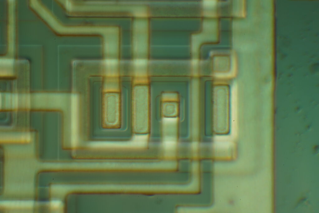
The most famous semiconductor is silicon. It's the second most abundant element in the Earth's crust, found in sand and quartz. To understand what makes silicon special, we need to look at how its atoms bond together.
A Crystal of Bonds
A silicon atom has four electrons in its outermost shell, called valence electrons. In a pure silicon crystal, each atom shares these four electrons with four neighboring atoms. This creates strong covalent bonds, forming a stable, orderly, and repeating three-dimensional structure called a crystal lattice.
In this arrangement, all the valence electrons are locked into bonds. Since there are no free-floating electrons to carry a current, pure silicon at very low temperatures acts like an insulator. To get it to conduct, we need to break some of these bonds and free up an electron.
But how much energy does that take? The answer lies in the concept of energy bands.
The Energy Gap
In a crystal, electrons can only exist at specific energy levels. These levels are grouped together into ranges, or "bands."
- Valence Band: The energy band where electrons are part of covalent bonds. They are attached to their atoms and cannot move to conduct electricity.
- Conduction Band: A higher energy band where electrons are free from their bonds. An electron in the conduction band can move through the crystal, carrying an electric current.
The space between these two bands is crucial. It’s called the bandgap.
Bandgap
noun
The minimum amount of energy required to excite an electron from the valence band into the conduction band, where it can participate in electrical conduction.
The size of the bandgap determines a material's electrical properties. Conductors have overlapping bands, so electrons can move freely with no extra energy. Insulators have a very large bandgap, making it extremely difficult for an electron to make the jump. Semiconductors have a small, manageable bandgap—just right for electronic applications.
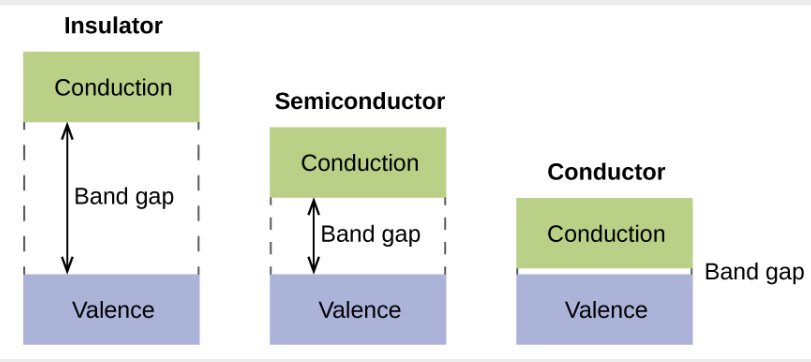
When an electron gains enough energy (from heat or light) to jump to the conduction band, it leaves behind an empty spot in the valence band. This empty spot is called a hole, and it acts like a positive charge. The movement of both free electrons and holes contributes to electrical current.
Adding Impurities
A pure semiconductor, like silicon, is called an intrinsic semiconductor. It doesn't conduct very well on its own because it relies on random thermal energy to create electron-hole pairs. To make semiconductors useful, we intentionally introduce impurities into the crystal lattice. This process is called doping, and it dramatically changes the material's conductivity.
A doped semiconductor is known as an extrinsic semiconductor.
Doping allows us to tailor the electrical properties of a semiconductor for specific tasks.
There are two types of doping:
N-type Doping: We add an element with five valence electrons, like phosphorus. Four of phosphorus's electrons form bonds with the surrounding silicon atoms, but the fifth electron is left over. This extra electron is not part of a bond and is free to move into the conduction band with very little energy. Since we've added negative charge carriers (electrons), we call this an N-type semiconductor.
P-type Doping: We add an element with three valence electrons, such as boron. When boron replaces a silicon atom in the lattice, it can only form three covalent bonds. This leaves one of its silicon neighbors with an un-bonded electron, creating a vacancy or a hole. This hole can easily accept an electron from a nearby bond, causing the hole to effectively move. Since we've added positive charge carriers (holes), we call this a P-type semiconductor.
By doping silicon to create N-type and P-type regions right next to each other, we can build fundamental electronic components. The boundary between these two regions, called a P-N junction, is the basis for diodes, transistors, and integrated circuits.
Ready to check your understanding?
What is the defining characteristic of a semiconductor material?
In a pure silicon crystal at very low temperatures, why does it behave like an insulator?
Understanding these core concepts—the atomic structure, the bandgap, and the effect of doping—is the first step to seeing how the digital world is built.