Semiconductor Supply Chain Risks
Semiconductor Supply Chain Overview
A Chip's Global Journey
Nearly every piece of modern technology, from your smartphone to your car, runs on semiconductors. These tiny electronic components, often called chips, are the brains of our digital world. But a single chip doesn't just appear out of thin air. It's the product of a long, incredibly complex, and globe-spanning supply chain.
This process is one of the most sophisticated manufacturing endeavors in human history. It requires immense capital, specialized knowledge, and international cooperation. Let's follow the journey of a semiconductor from raw material to a finished product, highlighting the key stages and the places where they happen.
From Sand to Silicon Wafer
The journey begins with basic raw materials. The most important is silicon, which is derived from quartz, a mineral found in common sand. However, not just any sand will do. It must be processed into extremely pure, electronics-grade silicon—often 99.9999999% pure. This material is then melted and grown into large, cylindrical crystals called ingots.
These ingots, which can weigh over 200 pounds, are sliced into perfectly thin discs called wafers. These wafers are the foundation upon which the intricate circuits of a semiconductor are built. While silicon is abundant, the process of refining it to this level of purity is highly specialized and energy-intensive. Key countries for sourcing and refining these raw materials include China, the United States, and Australia.
Fabrication and Assembly
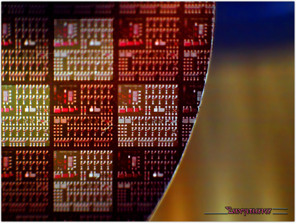
Next comes wafer fabrication, the most complex and expensive part of the process. In enormous, multi-billion dollar factories called "fabs," hundreds of chips are built up layer by layer on a single wafer. This involves a process called photolithography, where patterns of the chip's circuitry are repeatedly projected and etched onto the silicon.
This stage demands unbelievable precision. Fabs must be cleaner than hospital operating rooms, as a single speck of dust can ruin an entire batch of chips. Because of the immense cost and technical expertise required, wafer fabrication is highly concentrated. Taiwan (led by TSMC) and South Korea (led by Samsung) dominate the manufacturing of the most advanced chips, with the United States (led by Intel) also being a major player.
The circuits etched onto these wafers can have features that are thousands of times thinner than a human hair.
After fabrication, the wafer is sent to another facility for Assembly, Testing, and Packaging (ATP). Here, the wafer is cut into individual chips, or "dies." Each functional die is then placed into a protective plastic or ceramic package, and tiny wires are connected to its pins. Finally, every chip is tested to ensure it works correctly.
Unlike fabrication, ATP is more labor-intensive and is often done in different countries to save costs. Major hubs for this stage are found across Southeast Asia, particularly in Malaysia, Vietnam, and the Philippines, as well as in Taiwan and China.
This sophisticated global semiconductor chain has been made possible by decades of collaboration between companies in different countries.
The finished, packaged chips are then shipped to electronics manufacturers around the world. There, they are integrated into circuit boards and assembled into the final products we use every day, like laptops, servers, and medical devices. This final assembly stage is also globally distributed, with China being the largest hub for consumer electronics manufacturing.
From a grain of sand to the phone in your pocket, a single semiconductor travels the world, passing through the hands of highly specialized workers and companies at each step. This intricate global dance is what powers our modern digital economy.
Let's review what you've learned about this complex global journey.