Semiconductor Supply Chain Risks
Semiconductor Supply Chain Overview
The Backbone of Modern Tech
Nearly every piece of modern electronics, from your phone to your car, runs on semiconductors. These tiny electronic components, often called chips or integrated circuits, act as the brains of our devices. They are fundamental to how we live and work.
Semiconductors are the lifeblood of modern technology — from AI to cloud computing to self-driving cars.
But how does a sliver of silicon become the powerful engine inside a supercomputer? The answer lies in one of the most complex and globalized manufacturing processes ever created: the semiconductor supply chain. It's a journey that spans continents, involves hyper-specialized companies, and requires mind-boggling precision.
From Sand to Silicon Wafer
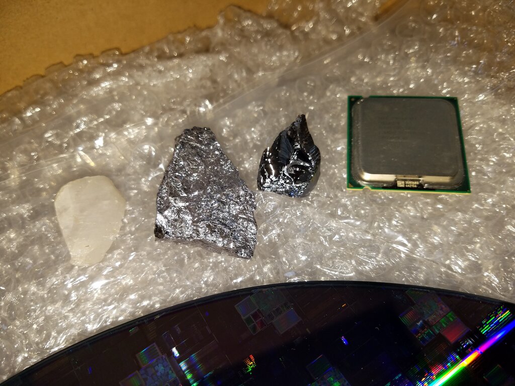
The journey begins with a surprisingly common material: sand. Specifically, high-purity quartz sand is the primary source of silicon, the element that forms the foundation of most semiconductors.
The raw quartz is melted down and purified in an intense process to create large, cylindrical single-crystal ingots. These ingots are almost 100% pure silicon. They are then sliced into ultra-thin discs called wafers, which are polished to a mirror-like finish. A single wafer, typically about the thickness of a credit card, will eventually hold hundreds or even thousands of individual chips.
Anatomy of the Supply Chain
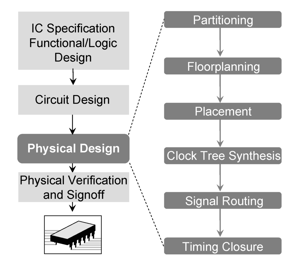
Creating a semiconductor is not a one-company job. The supply chain is a global network of specialists, each mastering a critical step in the process. We can break this journey into four main stages.
1. Design & IP Before a chip can be made, it must be designed. This is a highly intellectual process, like drawing up the blueprints for a skyscraper. "Fabless" companies specialize in designing chips without owning their own manufacturing plants. They create intricate layouts of billions of transistors. They also often license intellectual property (IP) cores, which are pre-designed blocks of circuitry, from other specialist firms to speed up development.
2. Fabrication This is where the design becomes a physical reality. The blueprints are sent to a foundry, or "fab," a multi-billion dollar factory. Inside the fab's cleanrooms, the wafers go through hundreds of steps. A process called photolithography is used to etch the transistor patterns onto the silicon, layer by microscopic layer. This is one of the most technologically advanced and capital-intensive manufacturing processes on Earth.
3. Assembly & Test Once the wafer is fully processed, it's cut into individual chips, or dies. Each die must then be packaged to protect it and connect it to the outside world. This involves placing the tiny silicon die into a protective casing and attaching pins that will eventually be soldered onto a circuit board. After packaging, every single chip is rigorously tested to ensure it works perfectly. Defective chips are discarded.
4. Final Product Integration Finally, the finished, tested chips are shipped to electronics companies around the world. These companies integrate the chips into their final products, like laptops, smartphones, cars, and medical equipment. This is the last step before the product reaches the consumer.
This entire chain is incredibly spread out. Chip design might happen in the United States, fabrication in Taiwan, and assembly and testing in Malaysia. This global specialization allows for incredible efficiency and innovation, but it also creates a deeply interconnected system where a disruption in one part of the world can affect the entire industry.
What is the primary raw material used as the source for the silicon in most semiconductors?
What is the primary function of a "fabless" company in the semiconductor supply chain?