Semiconductor Fabrication Essentials
Introduction to Semiconductors
The In-Between Material
In the world of electricity, materials usually fall into two camps. Conductors, like copper, let electricity flow freely. Insulators, like rubber, stop it completely. Semiconductors are the special materials that live in the middle. They can act like an insulator or a conductor, depending on the conditions.
semiconductor
noun
A solid substance that has a conductivity between that of an insulator and that of most metals, either due to the addition of an impurity or because of temperature effects.
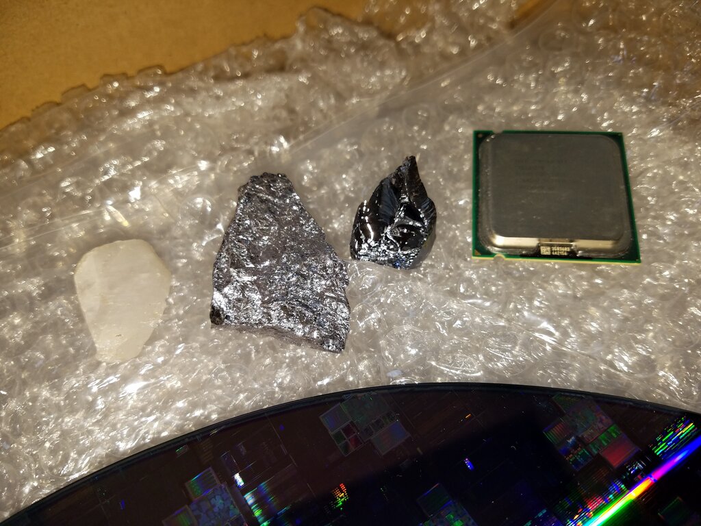
This ability to switch their conductivity is what makes them the foundation of modern electronics. From the processor in your phone to the sensors in a car, semiconductors are running the show. The most famous semiconductor material is silicon, which is made from sand.
The Energy Gap
To understand how semiconductors work, we need to look at their electrons. In any material, electrons exist at different energy levels, grouped into bands. The two most important bands are the valence band and the conduction band.
The valence band is where electrons are comfortably attached to their atoms. For electricity to flow, these electrons need to break free and move into the conduction band, where they can zip through the material.
The space between these two bands is called the band gap. It’s the amount of energy an electron needs to absorb to make the leap from the valence band to the conduction band.
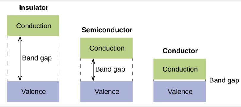
In a conductor, the bands overlap, so electrons move freely with very little energy. In an insulator, the band gap is huge, and it's almost impossible for electrons to make the jump. Semiconductors have a small, manageable band gap. A little bit of energy, perhaps from heat or light, is all it takes for an electron to get promoted to the conduction band.
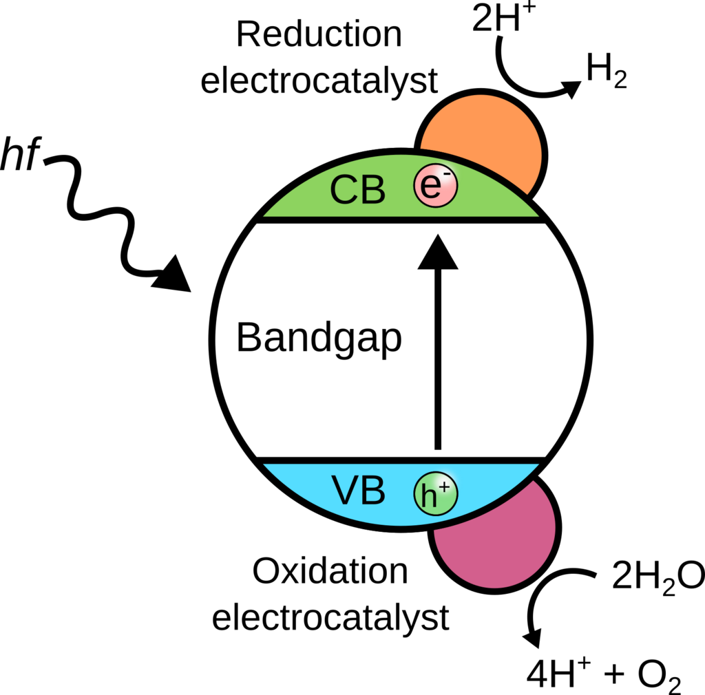
When an electron jumps, it leaves behind an empty spot in the valence band. This spot is called a hole, and it behaves like a positive charge. This creation of a mobile electron and a mobile hole is called an electron-hole pair, and both can help conduct electricity.
Pure vs. Doped
A perfectly pure semiconductor, like pure silicon, is called an intrinsic semiconductor. It doesn't conduct electricity very well at room temperature because not many electrons have enough energy to jump the band gap.
To make them more useful, we intentionally add tiny amounts of impurities to the semiconductor crystal. This process is called doping, and the resulting material is an extrinsic semiconductor. Doping dramatically changes the material's conductivity.
Doping is what gives us control over a semiconductor's electrical properties.
There are two types of doping, creating two types of extrinsic semiconductors.
N-type (Negative): We dope silicon with an element like phosphorus, which has five valence electrons (one more than silicon's four). Four of phosphorus's electrons bond with neighboring silicon atoms, but the fifth one is left over. This extra electron is loosely bound and can easily move to the conduction band, becoming a negative charge carrier.
P-type (Positive): We dope silicon with an element like boron, which has three valence electrons (one fewer than silicon). When boron bonds with silicon atoms, there's one spot missing an electron. This creates a hole, which acts as a positive charge carrier. An electron from a nearby atom can easily jump into this hole, causing the hole to move.
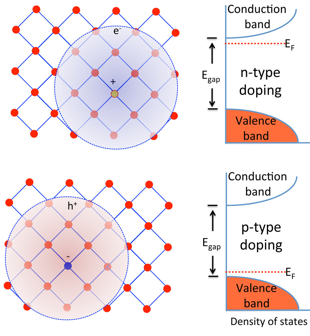
This ability to create materials with either an excess of electrons (N-type) or an excess of holes (P-type) is the key to building electronic devices. By joining P-type and N-type materials together, we can create diodes, transistors, and integrated circuits.
| Type | Description | Dopant Example (for Silicon) | Majority Charge Carrier |
|---|---|---|---|
| Intrinsic | Pure semiconductor | None | Electrons and Holes (equal) |
| N-type | Doped to add extra electrons | Phosphorus (P) | Electrons (-) |
| P-type | Doped to create holes | Boron (B) | Holes (+) |
Semiconductors are insulators capable of conducting electrons within a certain narrow energy band - a useful trick that makes integrated circuits and other electronics possible.
This control over conductivity is the foundation of every digital device we use today.
Ready to check your understanding?
What is the defining characteristic of a semiconductor material?
In the context of electron energy bands, what does the "band gap" represent?
By understanding these fundamentals, you can begin to see how simple materials like silicon are engineered to perform the complex calculations that power our world.