Semiconductor Charge Transport
Semiconductor Basics
The In-Between Material
Some materials, like copper, let electricity flow freely. They're called conductors. Others, like rubber, block it almost completely. They're insulators. Semiconductors are the fascinating materials that fall somewhere in between.
What makes them special isn't just their middle-ground conductivity, but our ability to precisely control it. To understand how, we need to look at electrons. In any solid material, electrons occupy specific energy levels, or "bands."
Think of it like floors in a building. Electrons usually hang out on the lower floors, called the valence band. To conduct electricity, they need to jump to a higher, empty floor called the conduction band. The space between these floors is the band gap.
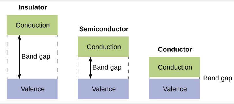
In conductors, the valence and conduction bands overlap. Electrons can move freely, like walking across a single, open-plan floor. In insulators, the band gap is huge. Electrons are stuck on the valence floor with no easy way to get to the conduction floor. Semiconductors have a small, manageable band gap. A little bit of energy, like from heat or light, is enough to get some electrons to make the jump.
Electrons and Holes
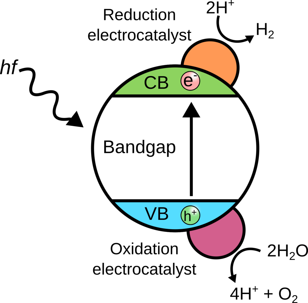
When an electron gets enough energy to jump from the valence band to the conduction band, it starts moving around and contributes to electrical current. But it also leaves something behind: an empty spot in the valence band.
hole
noun
The absence of an electron in the valence band of a semiconductor, which behaves like a positively charged particle.
This empty spot is called a hole. Because it represents the absence of a negative charge, a hole effectively has a positive charge. A nearby electron in the valence band can easily move into this hole, which causes the hole to move to the spot that electron just left. It's like a single empty seat in a crowded movie theater row. As people shift over one by one to let someone pass, the empty seat appears to travel down the row.
So, in a semiconductor, there are two types of charge carriers that create current: the negatively charged electrons in the conduction band and the positively charged holes moving through the valence band.
Pure vs. Impure
A perfectly pure semiconductor, like a crystal of pure silicon, is called an intrinsic semiconductor. At room temperature, thermal energy creates a small number of electron-hole pairs. But the number is balanced—for every free electron, there is one hole. This means intrinsic semiconductors aren't very good conductors on their own.
To make them useful, we introduce impurities. This process is called doping, and it creates what's known as an extrinsic semiconductor. Doping is the secret to modern electronics. It allows us to fine-tune a semiconductor's conductivity by creating a surplus of either electrons or holes.
The controlled manipulation of the charge carrier concentration in nanometer thin layers is the basis of current semiconductor technology and of fundamental importance for device applications.
The Power of Doping
Doping involves adding a tiny amount of a different element into the semiconductor's crystal lattice. Depending on the element used, we can create two types of extrinsic semiconductors.
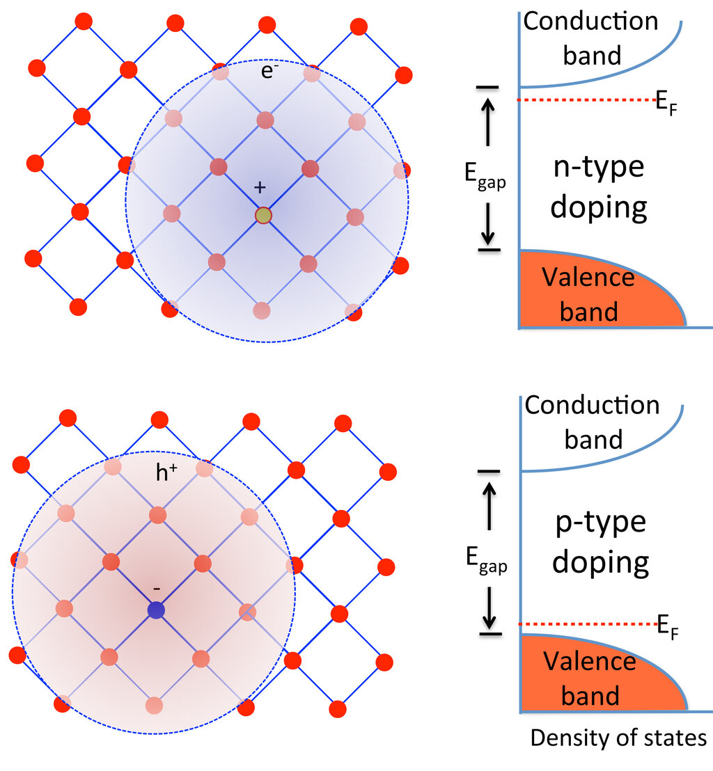
N-type Semiconductors To create an N-type (Negative-type) semiconductor, we dope silicon with an element that has five valence electrons, like phosphorus. Silicon atoms only have four. When a phosphorus atom replaces a silicon atom in the crystal, four of its electrons form bonds with neighboring silicon atoms. The fifth electron is left over and is only weakly attached. It takes very little energy to knock this electron loose, sending it into the conduction band without creating a hole in the valence band.
In N-type material, electrons are the majority carriers, and holes are the minority carriers.
P-type Semiconductors To create a P-type (Positive-type) semiconductor, we use an element with three valence electrons, like boron. When a boron atom sits in the silicon lattice, it can only form three bonds. This leaves one bond incomplete, creating a hole. This hole can easily accept an electron from a neighboring silicon atom, causing the hole to move. In this case, we've added holes without adding free electrons.
In P-type material, holes are the majority carriers, and electrons are the minority carriers.
By doping, we can increase a semiconductor's conductivity by a factor of thousands or even millions. More importantly, we can choose whether the current will be carried primarily by negative electrons or positive holes. This control is the fundamental principle that allows us to build diodes, transistors, and all the integrated circuits that power our world.
Let's check your understanding of these core concepts.
What property primarily determines whether a material is a conductor, an insulator, or a semiconductor?
In a semiconductor, what is a "hole"?
These concepts of electrons, holes, and doping are the essential building blocks for understanding how semiconductor devices work.