Professional PCB Design and Layout
Schematic Design Mastery
From Sketch to Blueprint
A schematic is more than just a drawing of a circuit. It's the foundational blueprint for a physical Printed Circuit Board (PCB). While a napkin sketch might capture the basic connections, a professional schematic communicates design intent with absolute clarity. This precision is vital because the schematic directly informs the next stage: creating the physical board layout.
The core principle of a schematic is to convey functional connectivity—which pin connects to which pin—without regard for the actual physical arrangement of these components in the final device.
For any design more complex than a simple blinking light, organisation is key. A messy, sprawling schematic is difficult to read, debug, and maintain. The goal is to create a document that is not only electrically correct but also logically structured, allowing anyone (including your future self) to understand the circuit's function at a glance.
Taming Complexity with Hierarchy
As designs grow, a single-page schematic becomes a tangled mess. The solution is hierarchical design. Think of it like a company's organisational chart. Instead of listing every employee on one page, you have departments, and within those, teams. In a schematic, you group related parts of the circuit into functional blocks, each on its own sheet.
Each of these blocks lives on a separate 'sheet', which is then referenced on the main or 'root' sheet. This modularity makes the design vastly easier to understand and reuse. The power supply you design for one project can be easily dropped into another.
To connect these sheets, we use nets. A net is simply a connection between two or more points. Connections within a single sheet are local nets. To connect between sheets, you need global nets or hierarchical labels. A global net, like GND or +5V, is accessible from any sheet in the design. They act as common buses for power and ground planes. For other inter-sheet signals, you use hierarchical labels, which function like doorways, passing a signal from a parent sheet to a child sheet.
From Symbol to Footprint
Every component in your schematic has two identities: its logical symbol and its physical footprint. The symbol is the abstract representation you work with in the schematic (e.g., the zig-zag for a resistor). The footprint is the pattern of copper pads on the physical PCB where the component will be soldered.
Modern design software, like , requires you to map each symbol to a specific footprint. A single resistor symbol, for instance, could be mapped to dozens of different footprints. Will it be a large, easy-to-solder through-hole resistor, or a tiny 0402 surface-mount component smaller than a grain of sand? This choice is a critical design decision.
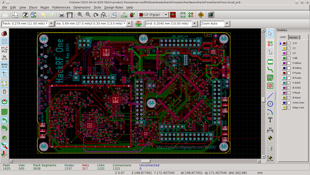
The primary choice is between Through-Hole Technology (THT) and (SMT). THT components have long leads that go through holes in the board and are soldered on the other side. SMT components have no leads; they are soldered directly onto pads on the board's surface.
| Feature | Through-Hole (THT) | Surface-Mount (SMT) |
|---|---|---|
| Size | Larger components, more board space | Smaller components, high density |
| Soldering | Easier to hand-solder, good for prototypes | Difficult to hand-solder tiny parts |
| Durability | Stronger mechanical bonds | Weaker mechanical bonds |
| Automation | Difficult to automate assembly | Ideal for automated assembly |
| Cost | Components can be cheaper, but assembly is costlier | Components can be pricier, but automated assembly is cheaper at scale |
Your choice depends on your project's needs. Are you building a one-off prototype by hand? Through-hole might be easier. Are you designing a compact device for mass production? SMT is the only practical option.
The Automated Sanity Check
Before you even think about laying out traces on a PCB, you must run an Electrical Rule Check (ERC). The ERC is an automated tool that functions like a proofreader for your schematic. It won't tell you if your circuit works logically, but it will catch a wide range of common connection errors.
The ERC tool checks your schematic for errors like unconnected pins, outputs connected together, or inputs that aren't driven by an output. It's your first line of defense against simple mistakes.
Common errors flagged by an ERC include:
- Unconnected Pins: A pin on a component that isn't connected to anything. Sometimes this is intentional, but often it's an oversight.
- Multiple Outputs Connected: Connecting two output pins together can cause a short circuit.
- Floating Inputs: An input pin that isn't connected to a defined voltage level, which can lead to unpredictable behaviour.
Fixing ERC errors at the schematic stage is trivial. Finding the same errors after the PCB has been manufactured is expensive and frustrating. Always run the ERC and resolve every warning before proceeding to the layout phase.
What is the primary function of a schematic in the electronics design process?
In a hierarchical schematic, what is the correct way to connect a signal, that is not a power net like +5V, from a main 'root' sheet to a component within a 'child' sheet?
With a clean, hierarchical, and error-checked schematic, you have a solid blueprint. Now you're ready to translate that logical design into a physical reality on the circuit board.