Printed Circuit Board Manufacturing Explained
PCB Materials
The Anatomy of a Circuit Board
A printed circuit board, or PCB, is the foundation of almost every electronic device. It looks like a complex city of metallic pathways, but at its core, it's a layered sandwich of simple materials. The three main ingredients are the substrate, the copper foil, and the prepreg that holds multi-layer boards together.
Think of the substrate as the board's skeleton. It provides the rigid structure. The copper foil is the nervous system, forming the conductive paths that allow electricity to flow. Let's break down these key components.
The Substrate
The substrate is the insulating material that makes up the bulk of the PCB. It needs to be a poor conductor of electricity to prevent the copper paths from short-circuiting. The most common substrate material by far is FR-4.
FR-4 is a woven fiberglass cloth impregnated with an epoxy resin that is flame retardant—that's what "FR" stands for. It's strong, reliable, and relatively inexpensive, making it the workhorse of the electronics industry for everything from toys to computers.
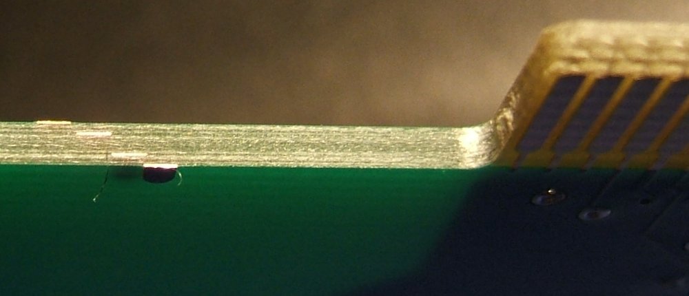
But not all electronics are rigid. Devices that need to bend or fit into tight spaces, like smartphones or medical implants, require flexible PCBs. For these, a different substrate is used, most commonly polyimide. This material is a high-performance plastic that can withstand high temperatures and can be bent repeatedly without breaking.
The choice of substrate directly impacts the board's physical properties, electrical performance, and cost.
The Copper Layer
Laminated onto the substrate is a thin sheet of copper foil. This is the conductive layer that gets etched away to create the traces, pads, and other features that guide electricity between components. The thickness of this copper layer is a critical parameter in PCB design.
Copper thickness is typically measured in ounces per square foot (oz/ft²). This might seem odd, but it's a standard way to describe the weight, and thus thickness, of the foil. A 1 oz copper board has enough copper to weigh one ounce if spread over a one-square-foot area. Most standard PCBs use 1 oz copper, but applications that handle a lot of electrical current might require thicker 2 oz or 3 oz copper to prevent overheating.
| Copper Weight (oz/ft²) | Approx. Thickness (mils) | Approx. Thickness (µm) |
|---|---|---|
| 0.5 oz | 0.7 | 18 |
| 1 oz | 1.4 | 35 |
| 2 oz | 2.8 | 70 |
Binding the Layers
Simple PCBs might have copper on just one or two sides. But complex devices like motherboards can have a dozen or more layers stacked on top of each other. To bind these layers into a single, solid board, manufacturers use a material called prepreg.
Prepreg
noun
A sheet of fiberglass that has been pre-impregnated with a resin system. The resin is partially cured and acts as a glue when heated and pressed.
During manufacturing, layers of copper-clad substrate are alternated with sheets of prepreg. This whole stack is then placed in a powerful press that applies intense heat and pressure. The heat melts the epoxy in the prepreg, which flows and fills any gaps. As it cools, the epoxy cures and hardens, permanently bonding the layers together to form a solid, multi-layer laminate.
These materials—substrate, copper, and prepreg—form the fundamental structure of every PCB. Their specific properties and how they are combined determine the board's final performance, durability, and capabilities.
Let's check your understanding of these foundational materials.
What is the primary function of the substrate in a printed circuit board?
An engineer is designing a wearable device that needs to bend around a user's wrist. Which substrate material would be the most suitable choice?
Understanding these materials is the first step in grasping how a simple design becomes a functional electronic circuit.