Printed Circuit Board Manufacturing
PCB Basics
The Skeleton of Electronics
Nearly every electronic device you own, from your phone to your microwave, has a Printed Circuit Board, or PCB, inside. These boards are the foundation of modern electronics, providing a physical structure and electrical connections for all the tiny components that make a device work.
PCB
noun
A board made of non-conductive material with conductive lines printed or etched onto it, used to mechanically support and electrically connect electronic components.
Think of a PCB as a miniature, highly organized city for electricity. Instead of roads for cars, it has copper pathways called traces that guide electrical signals between different components. This eliminates the messy, unreliable “point-to-point” wiring that was common in early electronics, which looked like a tangled mess of spaghetti.
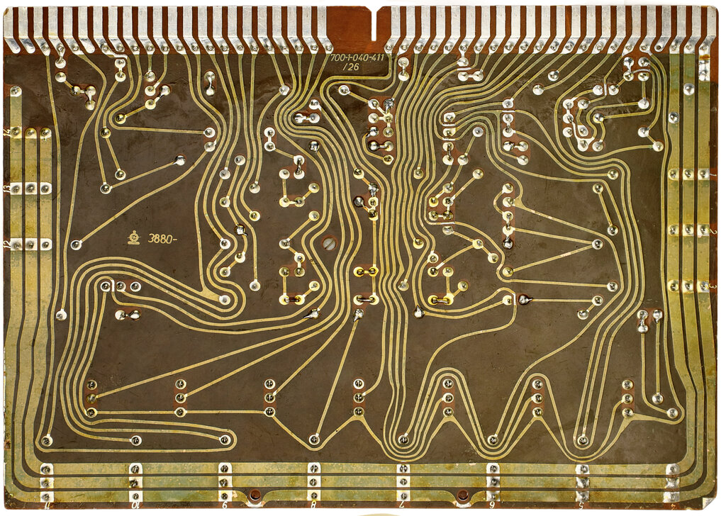
By creating a fixed, repeatable layout, PCBs make it possible to mass-produce complex electronic devices reliably and affordably. They are the unsung heroes that bring our digital world to life.
Anatomy of a Board
At its simplest, a PCB is a sandwich of different materials. The main body, called the substrate, is usually made from a rigid fiberglass material like FR-4. It provides insulation, so electricity only flows where we want it to. A thin layer of copper is laminated onto this substrate. We then etch away unwanted copper, leaving behind the precise network of traces that form the circuit.
Key features of a PCB include:
- Layers: The sheets of substrate and copper that make up the board.
- Traces: The copper pathways that act as wires.
- Pads: Exposed areas of copper where components are soldered to the board.
- Vias: Plated holes that connect traces on different layers of the board. Think of them as tiny elevators for electricity.
Via
noun
A plated hole in a printed circuit board that allows a trace to pass from one layer to another.
Types of PCBs
PCBs aren't one-size-fits-all. They come in various forms, tailored to the needs of the device they will power. The differences usually come down to the number of layers and the flexibility of the substrate material.
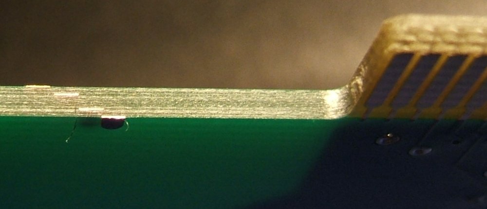
The main categories you'll encounter are single-sided, double-sided, and multi-layer boards. As electronics become more complex and compact, like in smartphones and laptops, multi-layer boards are essential. They stack multiple circuits on top of each other, creating a dense, three-dimensional electrical highway.
More layers allow for more complex and compact circuits, but they also increase the cost and manufacturing difficulty.
Boards can also be rigid or flexible. While most PCBs are stiff (rigid), some applications require circuits that can bend or fold. Flexible PCBs, made from materials like polyimide, can be found in cameras, wearable tech, and other devices where space is tight or movement is required.
| Type | Description | Common Use |
|---|---|---|
| Single-Layer | Circuit on one side of the substrate. | Simple electronics, calculators |
| Double-Layer | Circuits on both sides of the substrate. | Power supplies, LED lighting |
| Multi-Layer | Multiple circuit layers laminated together. | Smartphones, computers |
| Rigid | Made from a solid, inflexible substrate. | Most consumer electronics |
| Flexible | Made from a bendable material. | Wearables, medical devices |
Time to check what you've learned.
In a multi-layer PCB, what is the primary function of a via?
If a PCB is compared to a miniature city, what do the copper traces represent?
Understanding these basic building blocks is the first step in appreciating the intricate design and engineering that goes into every piece of modern technology.