Physical Design for Semiconductor Chips
Introduction to Physical Design
From Blueprint to Reality
Imagine an architect has designed a revolutionary new skyscraper. They have detailed blueprints showing every room, floor, and function. But those plans don't specify exactly where each steel beam, electrical wire, or plumbing pipe should be placed for maximum efficiency and structural integrity. That's a separate, highly detailed job. In chip design, that job is called physical design.
Physical design is the process of transforming a circuit's logical blueprint into an actual, physical layout that can be manufactured. The initial design, often written in a hardware description language, explains what the chip does. Physical design figures out how to build it on a tiny piece of silicon, arranging millions or billions of components and wiring them together.
This stage is critical. A brilliant logical design can fail completely if the physical layout is poor, leading to a chip that's slow, overheats, or simply doesn't work.
The Journey from Code to Silicon
The entire journey from an abstract idea to a manufacturable file is often called the "RTL to GDSII" flow. Let's break down what that means.
RTL
noun
Stands for Register-Transfer Level. This is a high-level model of a digital circuit, written in a hardware description language like Verilog or VHDL. It describes how data moves between registers and the logical operations performed on that data.
Think of RTL as the functional specification. It's the starting point for physical design. The end goal is a file format called GDSII.
GDSII
noun
A database file format that has become the industry standard for data exchange of integrated circuit layouts. It contains the geometric shapes, text labels, and other information for every layer of the chip.
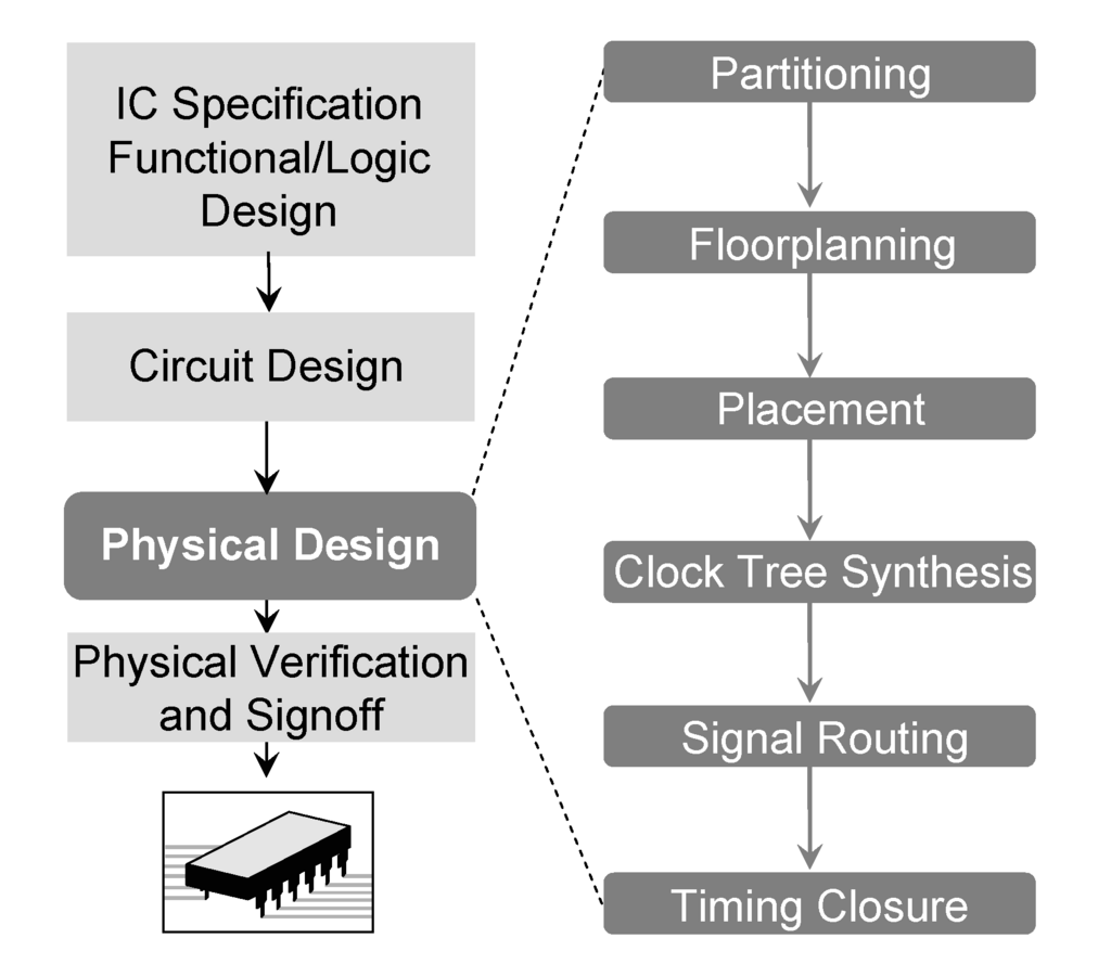
The GDSII file is the final instruction manual sent to the manufacturing plant, or "foundry," telling their machines exactly how to build the chip, layer by microscopic layer. The physical design process is the entire sequence of steps that converts the RTL into the GDSII.
The Three Big Goals
Throughout the physical design process, engineers are constantly balancing three competing objectives, known in the industry as PPA.
| Objective | What It Means | Why It Matters |
|---|---|---|
| Performance | How fast the chip can operate. | Determines the processing speed of a device. A faster chip means a snappier phone or a more powerful server. |
| Power | How much energy the chip consumes. | Lower power means longer battery life for mobile devices and reduced electricity costs and heat for data centers. |
| Area | How much silicon the chip occupies. | A smaller chip costs less to manufacture, allowing more chips to be cut from a single silicon wafer. |
The challenge is that improving one of these metrics often hurts another. For example, making a chip faster (better performance) might require larger transistors, which increases both area and power consumption. The art of physical design lies in finding the optimal balance for the chip's intended application.
Tools of the Trade
Manually arranging billions of transistors is impossible. This entire process relies on sophisticated software known as Electronic Design Automation (EDA) tools. These tools automate the complex tasks of placing components and routing the connections between them.
Companies like Cadence Design Systems, Synopsys, and Siemens EDA are the leaders in this field. Cadence, for example, offers a suite of tools that covers the entire physical design flow. Their Innovus Implementation System is a cornerstone for chip implementation, handling everything from placement and routing to timing and power optimization. These tools help engineers navigate the PPA trade-offs and verify that the final design will work correctly before it's sent off for the expensive manufacturing process.
Let's review the key concepts we've covered.
Ready to check your understanding?
What is the primary goal of the physical design process in chip manufacturing?
An engineer makes a design change that increases a chip's clock speed but also increases its size and heat output. This is an example of a trade-off between which factors?
Now that you understand the what and why of physical design, we can begin to explore the specific stages of this fascinating journey from a logical idea to a physical reality.