PCB Design Essentials
Introduction to PCB Design
The Electronic Skeleton
Nearly every electronic gadget you own, from your phone to your television, has a Printed Circuit Board (PCB) inside. It's the foundation of modern electronics, a rigid board that holds all the tiny components in place and connects them so they can work together. Think of it like a city. The components are the buildings—the houses, offices, and factories. The PCB itself is the land, and the thin copper lines etched onto it are the roads, power lines, and plumbing that connect everything, allowing electricity and information to flow.
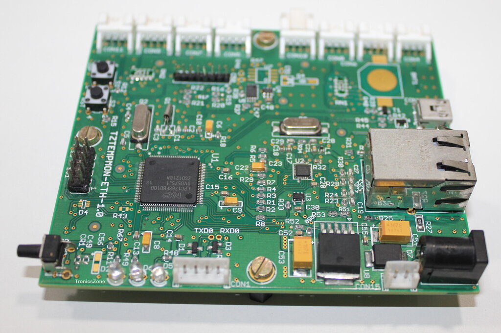
A bare PCB has a few key layers, each with a specific job.
| Layer | Purpose |
|---|---|
| Substrate | The base material, often made of fiberglass (FR-4), providing rigidity. |
| Copper | A thin layer laminated to the substrate, etched to create the conductive pathways, or traces. |
| Solder Mask | The green (or blue, red, etc.) coating that insulates the copper traces from accidental contact. |
| Silkscreen | The white letters and symbols printed on top, which help identify components and test points. |
The Building Blocks
A bare board is just the start. To bring a circuit to life, you need to add components. These are the individual electronic parts that perform specific tasks, like resisting current, storing charge, or processing information. While there are thousands of different components, most boards feature a few common types.
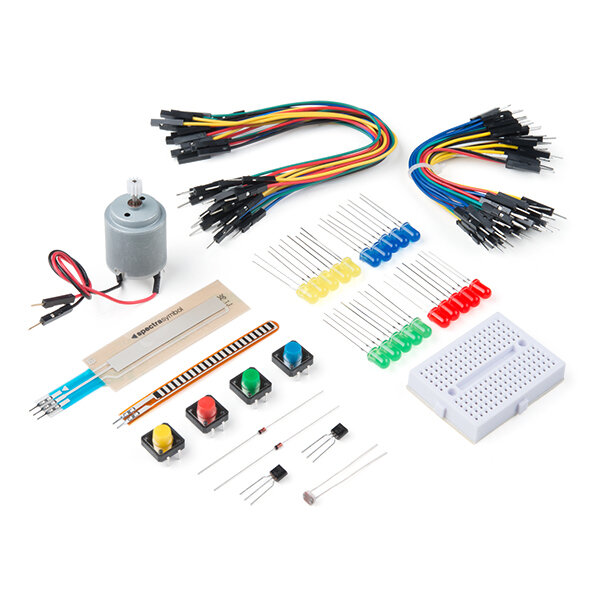
You'll almost always find resistors, capacitors, and connectors. The most complex components are Integrated Circuits, or ICs, which are essentially miniaturized circuits of their own.
Integrated Circuit
noun
A set of electronic circuits on one small flat piece (or "chip") of semiconductor material, usually silicon.
Components are attached to the board in one of two ways: they either pass through the board or sit on top of it.
From Idea to Layout
How do you know where all those components and traces are supposed to go? The process starts with a blueprint called an electrical schematic.
A schematic is a diagram that shows how the components in a circuit are electrically connected. It uses standardized symbols for each component and lines to show the connections between them. Crucially, a schematic shows what connects to what, but it doesn't show the physical size, shape, or location of the parts.
A schematic is like a recipe's ingredient list and instructions, while the final PCB is the finished dish.
Once the schematic is finalized, the designer moves on to the PCB layout. This is where the virtual components are placed onto a virtual board and the copper traces are routed between them. This entire process, from schematic to layout, is done using specialized software called Electronic Design Automation (EDA) tools.
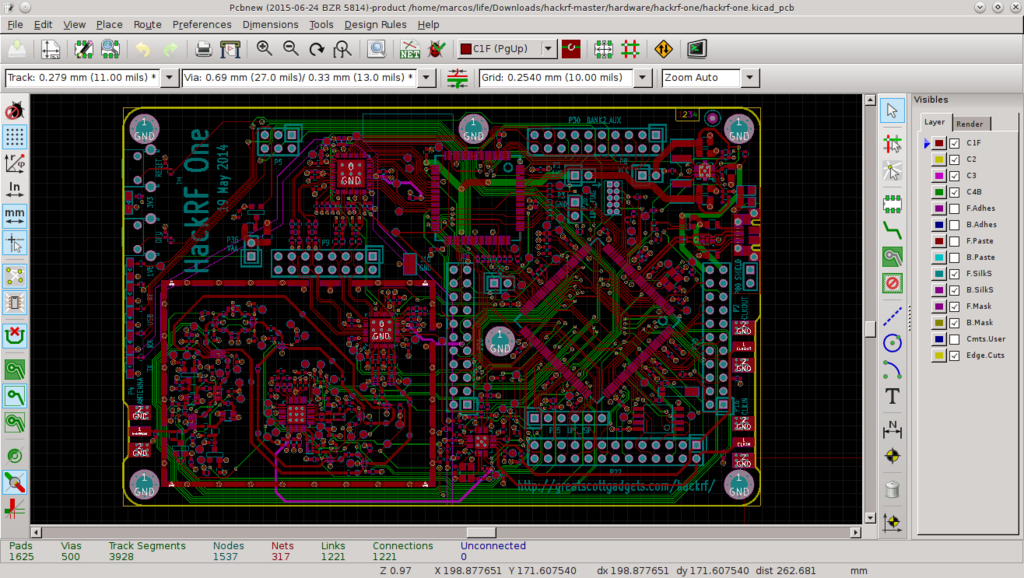
Popular EDA software includes KiCad (which is free and open-source), Autodesk Eagle, and Altium Designer. These powerful programs allow designers to draw the schematic, arrange the components on the board, define the rules for the design (like how close traces can be), and ultimately generate the files needed to manufacture the physical PCB.
Now that you understand the basics, let's test your knowledge.
What is the primary role of a Printed Circuit Board (PCB) in an electronic device?
Which of the following describes the purpose of an electrical schematic in the PCB design process?
Understanding these core concepts—what a PCB is, what it's made of, and how it's designed—is the first step into the world of electronics engineering.