P-N Diode Junction Potential Explained
Semiconductor Basics
The Heart of Electronics
At the core of every smartphone, computer, and modern gadget lies a special class of materials: semiconductors. As their name suggests, they are somewhere between a conductor, like copper, which lets electricity flow easily, and an insulator, like rubber, which blocks it almost completely. The most famous semiconductor is silicon, the second most abundant element in the Earth's crust.
What gives a material its electrical properties is how its electrons are arranged. Electrons exist in energy levels, or bands. For electricity to flow, electrons must be free to move. They can do this by jumping from a lower energy band, called the valence band, to a higher one, called the conduction band. The space between these bands is the band gap.
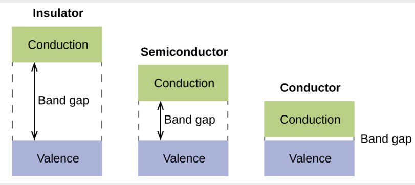
In conductors, the bands overlap, so electrons move freely. In insulators, the band gap is so large that electrons are stuck in the valence band. Semiconductors have a small, manageable band gap. A little energy can kick an electron up to the conduction band, allowing it to move and conduct electricity. This unique property is what we exploit to build electronic devices.
Pure and Simple
A perfectly pure semiconductor is called an intrinsic semiconductor. In its pure state, like a flawless crystal of silicon, it's not a very good conductor. At extremely cold temperatures, it acts like an insulator. But as it warms up, thermal energy can excite some electrons.
When an electron in the valence band gains enough energy, it jumps across the band gap into the conduction band. Now it's a free electron, able to carry an electric current. But it leaves something behind.
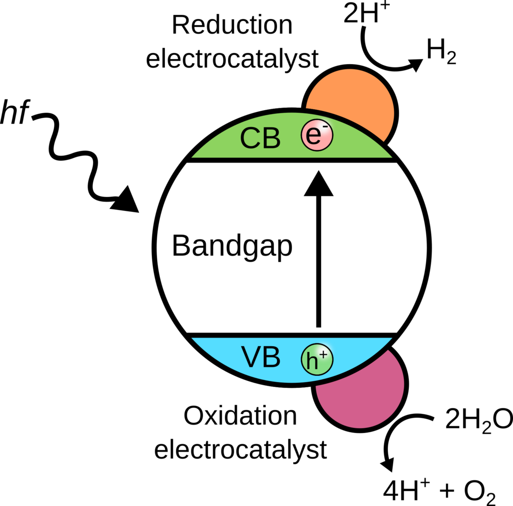
The empty spot it vacated in the valence band is called a hole. A hole isn't a physical particle; it's the absence of an electron. But this absence behaves like a positive charge. A nearby electron can move into the hole, which makes the hole appear to move in the opposite direction. So, in an intrinsic semiconductor, we have two types of charge carriers: free electrons (negative) and holes (positive). The number of free electrons is always equal to the number of holes.
In an intrinsic semiconductor, the concentration of free electrons () is equal to the concentration of holes (). This is often written as , where is the intrinsic carrier concentration.
Making Semiconductors Useful
Intrinsic semiconductors are interesting, but their low conductivity makes them impractical for most electronics. To change this, we intentionally introduce impurities into the semiconductor crystal. This process is called doping.
Doping
noun
The process of intentionally introducing impurities into an intrinsic semiconductor to alter its electrical properties.
Doping creates an extrinsic semiconductor. By adding tiny, controlled amounts of specific elements, we can dramatically increase the number of either free electrons or holes, making the material much more conductive. This gives us two new types of materials: N-type and P-type semiconductors.
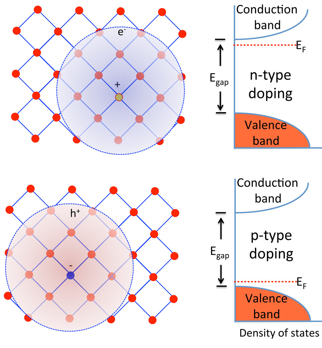
For N-type (Negative-type) material, we dope silicon with an element that has five valence electrons, like phosphorus. Silicon atoms have four valence electrons, which they use to form bonds with their neighbors. When a phosphorus atom replaces a silicon atom, four of its electrons form bonds, but the fifth is left over. This extra electron is loosely bound and can easily jump into the conduction band, becoming a free charge carrier. In N-type material, electrons are the majority carriers and holes are the minority carriers.
For P-type (Positive-type) material, we use an element with three valence electrons, like boron. When a boron atom replaces a silicon atom, it can only form three bonds. This leaves a vacancy, or a hole, in the fourth bond. This hole can easily accept an electron from a neighboring atom, causing the hole to move. In P-type material, holes are the majority carriers and electrons are the minority carriers.
The ability to create both N-type and P-type materials is the foundation of modern electronics. By joining these two types of materials, we can build diodes, transistors, and all the complex integrated circuits that power our world.
What characteristic of a material primarily determines its classification as a conductor, insulator, or semiconductor?
To create a P-type semiconductor, a pure silicon crystal is doped with an element that has three valence electrons, such as boron.