Navigating Semiconductor Supply Chain Risks
Semiconductor Supply Chain Overview
The Silicon Heartbeat
At the core of nearly every modern electronic device is a tiny piece of engineered material called a semiconductor. You can think of it as an incredibly sophisticated light switch. It can be turned on to allow electric current to flow, or off to stop it. By controlling these on/off states in billions of tiny switches, called transistors, on a single chip, we can perform complex calculations and store information.
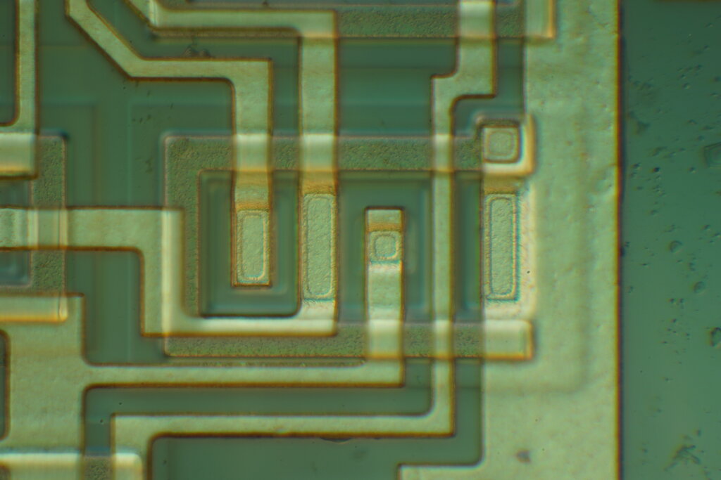
These chips are the brains behind our smartphones, computers, cars, and even refrigerators. They are fundamental to telecommunications, healthcare, and military systems. Without semiconductors, the digital world as we know it would not exist. Their creation, however, is one of the most complex and globalized manufacturing processes ever developed.
From Sand to Smartphone
The journey of a semiconductor is a marvel of global collaboration and precision engineering. It begins with one of the most common materials on Earth and ends with a device of unimaginable complexity. The process can be broken down into several key stages, each often occurring in a different part of the world.
1. Raw Materials & Equipment: The journey starts with high-purity silicon, which is refined from common sand (silicon dioxide). This silicon is grown into large, cylindrical crystals called ingots, which are then sliced into thin, perfectly polished discs known as wafers. This stage also includes the manufacturing of highly specialized equipment needed for chipmaking, such as lithography machines.
2. Design: Before a chip can be made, it must be designed. Specialized firms, known as "fabless" companies, create the intricate blueprints for the chip's circuitry using Electronic Design Automation (EDA) software. This design is a digital file containing billions of transistors and their connections.
3. Fabrication: This is the most capital-intensive step. The design blueprint is transferred onto the silicon wafers in massive, ultra-clean factories called foundries or fabs. The process, called photolithography, involves repeatedly projecting light through a template (a mask) to etch the circuit patterns onto the wafer. Hundreds or thousands of identical chips are built up in layers on a single wafer.
4. Assembly, Test, and Packaging (ATP): After fabrication, the wafer is cut into individual chips (called dies). Each die is tested, then encased in a protective package with metal pins that allow it to connect to a circuit board. This work is often done by specialized companies known as Outsourced Semiconductor Assembly and Test (OSAT) providers.
5. Final Product Integration: Finally, the packaged and tested chips are shipped to electronics manufacturers around the world. They are soldered onto circuit boards and integrated into the final products we use every day, like laptops, cars, and medical devices.
A Global Assembly Line
No single country dominates the entire semiconductor supply chain. Instead, it's a web of specialization, with different regions excelling at different stages. This global interdependence is a defining feature of the industry.
A chip designed in the United States might be fabricated in Taiwan using Dutch machinery, then sent to Malaysia for packaging before being installed in a German car.
This distribution of labor has allowed for incredible efficiency and innovation. Companies can focus on what they do best, whether it's designing the most powerful processors or manufacturing them at an immense scale with near-perfect quality.
| Region/Country | Area of Specialization |
|---|---|
| United States | Chip Design (EDA & Fabless), Specialized Equipment |
| Taiwan | Advanced Fabrication (Foundries) |
| South Korea | Memory Chip Fabrication (IDMs) |
| Japan | Raw Materials (Wafers, Chemicals), Equipment |
| Europe (esp. Netherlands) | Extreme Ultraviolet (EUV) Lithography Equipment |
| China | Assembly & Packaging, Maturing Fabrication |
| Southeast Asia (esp. Malaysia) | Assembly, Test, & Packaging (ATP) |
The companies involved also fall into distinct categories. Fabless companies like NVIDIA or Qualcomm focus solely on design. Foundries like TSMC are pure-play manufacturers that build chips for fabless companies. And Integrated Device Manufacturers (IDMs) like Intel and Samsung design and manufacture their own chips.
This sophisticated global semiconductor chain has been made possible by decades of collaboration between companies in different countries.
This intricate, globalized system allows for the continuous advancement of technology, but it also creates a unique set of challenges and dependencies across the world.
Let's check your understanding of the semiconductor supply chain.
What is the fundamental raw material used to create the silicon wafers for semiconductors?
A company that designs its own chips but outsources the manufacturing process to a specialized factory is known as what?
The semiconductor supply chain is a testament to modern engineering and global cooperation, turning a simple raw material into the engine of our digital lives.