Modern Computer Architecture and System Integration
Modern Processor Architecture
The Cache Hierarchy
A modern CPU core operates at blistering speeds, executing billions of cycles per second. System RAM, by comparison, is incredibly slow. If a processor had to wait for RAM to fetch every single piece of data it needed, the entire system would grind to a halt. This speed difference is often called the 'memory wall'.
To bridge this gap, processors use a multi-level cache system. Think of it like a workshop. The CPU is the craftsperson, and the data are the tools. System RAM is a large warehouse across town. It holds every tool, but fetching one takes a long time.
Cache is a small, extremely fast memory buffer located directly on the processor die. It stores frequently used data, so the CPU doesn't have to make the long trip to RAM.
This system is broken into hierarchical levels:
- Level 1 (L1) Cache: This is the smallest and fastest cache, like a tool belt. It's dedicated to a single CPU core and is typically split into two parts: an instruction cache (for program code) and a data cache (for the data the code is working on). L1 cache holds the data the CPU is most likely to need in the very next moment.
- Level 2 (L2) Cache: Larger and slightly slower than L1, this is like a personal toolbox right next to the workbench. It's also usually exclusive to a single core and serves as a buffer for the L1 cache. If the data isn't in L1, the CPU checks L2 before looking further.
- Level 3 (L3) Cache: This is the largest and slowest level of cache, like a shared tool cabinet in the workshop. The L3 cache is shared across all cores on the CPU. It not only holds data that multiple cores might need, but it also provides a fast way for cores to communicate with each other without going to main memory.
When the CPU needs data, it checks L1 first. If it's not there (a 'cache miss'), it checks L2, then L3. Only if it misses in all three caches does it make the slow journey to system RAM. This hierarchy ensures the most frequently used data is always just a few nanoseconds away.
The Modern Chip Layout
In the past, motherboards used a chipset composed of two main chips: the Northbridge and the Southbridge. The Northbridge was the high-speed traffic controller, connecting the CPU to RAM and the graphics card. The Southbridge handled slower communications for things like USB ports, hard drives, and audio.
This design had a bottleneck. All communication between the CPU and its most critical partners, RAM and the GPU, had to go through a separate chip. This introduced latency. Modern processors solve this by integrating those critical functions directly onto the CPU die. This design is called a System on Chip (SoC).
Today, the memory controller and the controller for high-speed PCIe lanes are built directly into the CPU. This gives the processor a direct, low-latency connection to RAM and high-bandwidth devices like graphics cards and NVMe solid-state drives. The separate chipset still exists (often called the Platform Controller Hub or PCH on Intel systems), but its role is now limited to managing the slower I/O, like USB ports and SATA drives.
Pipelines and Parallelism
Beyond physical layout, modern CPUs use sophisticated techniques to process instructions more efficiently. The core of this is the instruction pipeline. Instead of processing one instruction from start to finish before starting the next (Fetch -> Decode -> Execute -> Write Back), a pipelined processor works like an assembly line. While one instruction is being executed, the next one is being decoded, and the one after that is being fetched.
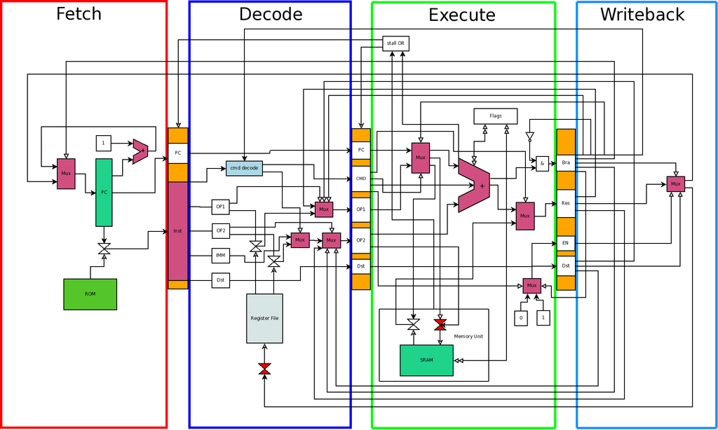
This dramatically increases throughput, which is the number of instructions completed per unit of time. The overall design of this pipeline, along with other features like branch prediction (guessing the outcome of an if/then statement to keep the pipeline full) and out-of-order execution (rearranging instructions to avoid stalls), is known as the processor's . It's the blueprint that defines how a CPU core actually gets work done, and it's why two processors with the same clock speed and core count can have vastly different performance.
Understanding this interplay of cache, integrated controllers, and efficient instruction processing is key to grasping why modern systems are so fast. It's not just about raw speed, but about smart, efficient design that minimizes waiting and maximizes work.
What is the primary problem that a multi-level CPU cache is designed to solve?
In the workshop analogy, which cache level is described as a 'shared tool cabinet' used by all CPU cores?