Mastering Digital Logic Synthesis
Logic Family Physics
From Theory to Silicon
Abstract logic gates are useful, but they don't exist in a vacuum. To build a real computer, these gates must be physically constructed from electronic components. The most fundamental of these is the transistor, a tiny semiconductor switch.
Groups of transistors arranged in specific ways to perform logic functions are called logic families. For decades, two families have dominated digital electronics: TTL (Transistor-Transistor Logic) and CMOS (Complementary Metal-Oxide-Semiconductor). While TTL was foundational for early digital systems, CMOS is the undisputed standard today, used in everything from microprocessors to memory chips.
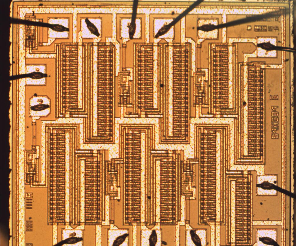
Understanding these families isn't just about history; it's about the practical engineering trade-offs that dictate how circuits are designed. Their differences in voltage levels, power consumption, and signal integrity determine the performance and efficiency of every digital device.
Defining High and Low
In the world of digital logic, 1s and 0s are not abstract concepts but specific voltage ranges. A logic gate doesn't output a perfect 5 volts for a 'high' signal or 0 volts for a 'low'. Instead, it operates within acceptable ranges or thresholds. These are defined by four key parameters:
- (Voltage Output High): The minimum voltage a gate will output for a logic 'high'.
- (Voltage Output Low): The maximum voltage a gate will output for a logic 'low'.
- (Voltage Input High): The minimum voltage an input must receive to be reliably interpreted as a logic 'high'.
- (Voltage Input Low): The maximum voltage an input can receive and still be reliably interpreted as a logic 'low'.
Any voltage between and is in an undefined or forbidden region. A signal in this range can cause unpredictable behavior in the logic gate, so designers work to ensure this never happens.
| Parameter | 5V TTL | 3.3V CMOS |
|---|---|---|
| (min) | 2.4 V | 2.4 V |
| (max) | 0.4 V | 0.4 V |
| (min) | 2.0 V | 1.5 V |
| (max) | 0.8 V | 0.8 V |
The gap between what a gate outputs and what the next gate requires as input is crucial. This gap is called the noise margin.
Noise margin is the buffer zone that protects the signal from small, unwanted voltage fluctuations, known as noise. This noise can come from nearby signals, power supply variations, or external interference. A larger noise margin means the circuit is more robust and less likely to misinterpret a signal.
For 5V TTL, both noise margins are 0.4 V. For 3.3V CMOS, the high margin is 0.9 V and the low margin is 0.4 V. The larger margin in CMOS is one reason it's more resilient to noise.
Practical Circuit Limits
Beyond voltage levels, other physical properties limit how gates can be connected. Two of the most important are fan-out and power dissipation.
Fan-out
noun
The maximum number of logic inputs that the output of a single logic gate can reliably drive.
Imagine a teacher speaking to a class. With a few students, her voice is easily heard. But in a massive lecture hall with hundreds of students, her voice might not carry. The gate's output is like the teacher's voice, and the inputs it's connected to are the students.
In TTL, fan-out is limited by the output's ability to source or sink current. In CMOS, the limitation is different. CMOS inputs have very high impedance, meaning they draw almost no current. Instead, the limit is capacitive loading. Each input acts like a tiny capacitor that must be charged or discharged every time the signal switches. The more inputs you connect, the more capacitance the output has to drive, and the slower the signal will switch.
The other critical factor is power. How much energy does a gate consume just by being on, and how much does it use when actively switching?
This is where the most significant difference between TTL and CMOS appears. A TTL gate is built with resistors that constantly draw current, whether its output is high or low. This results in significant static power dissipation—power consumed even when the circuit is idle.
CMOS architecture is fundamentally different. An inverter, the simplest logic gate, is made of two complementary transistors: a PMOS transistor connected to the power supply () and an NMOS transistor connected to ground. In a stable state (either high or low), one of these transistors is 'on' and the other is 'off', creating an open circuit. Almost no current flows, resulting in nearly zero static power dissipation.
However, CMOS does consume power when it's switching. This is called dynamic power dissipation. Every time the output switches from high to low or low to high, the small capacitance of the connected inputs and wiring must be charged or discharged. This movement of charge requires energy, and the faster the circuit switches, the more power it consumes.
This formula reveals why lowering the operating voltage is so effective at reducing power consumption in modern processors, and why high-frequency chips generate so much heat. The near-zero static power of CMOS is the primary reason it became the dominant technology for integrated circuits. It allows for billions of transistors to be packed onto a single chip without it melting from idle power draw.
Which logic family is the dominant standard for modern digital electronics, like microprocessors and memory chips, primarily due to its extremely low static power consumption?
In the context of logic gate voltage levels, what does the parameter (Voltage Input High) define?