Introduction to the EDMR Technique
Introduction to EDMR
A More Sensitive Look
Imagine trying to find a single faulty wire in a huge, complex circuit board. It's a tiny flaw, but it can cause the whole system to fail. In the world of materials science, especially with semiconductors, scientists face a similar challenge. They need to find and identify minuscule defects—sometimes just a handful of atoms—that can ruin an electronic device.
This is where Electrically Detected Magnetic Resonance (EDMR) comes in. It's a powerful technique that acts like a highly sensitive detective for the atomic world. At its core, EDMR is a way to study electron spins. As you might recall, an electron's spin creates a tiny magnetic moment. When placed in a strong magnetic field, these spins can align with or against the field.
By applying microwaves at a specific frequency, we can cause these electron spins to flip. Standard techniques, like Electron Spin Resonance (ESR), detect this flip by measuring the tiny amount of microwave energy the sample absorbs. EDMR does something different. Instead of looking for absorbed energy, it measures a change in the material's electrical resistance or current. This electrical signal is much easier to detect, making EDMR thousands of times more sensitive than traditional methods.
This electrical detection is the key. When a spin flips, it can briefly alter how electrons move through the material, causing a tiny, temporary blip in the current. By precisely measuring this blip, scientists can identify the chemical nature of the defect and even its location.
Historical Development
EDMR wasn't invented out of the blue. It grew from the foundations of Electron Spin Resonance (ESR), a technique developed in the 1940s. While ESR was revolutionary, scientists working with semiconductors in the 1960s and 70s hit a wall. They were trying to study defects in silicon, but the number of defects was often too small for ESR to detect.
Researchers realized that the properties they cared about most in a semiconductor—its electrical properties—could be used for detection. The first EDMR experiments showed that monitoring the conductivity of silicon while performing an ESR experiment provided a much stronger signal. This breakthrough opened the door to studying subtle defects that were previously invisible.
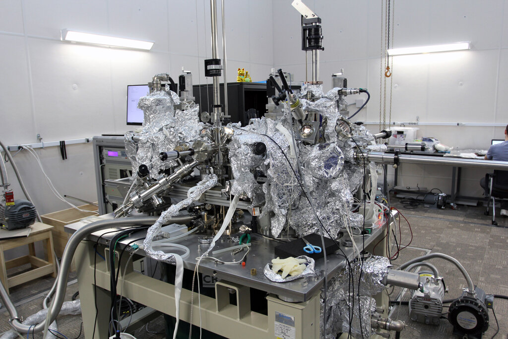
Over the years, the technique was refined, becoming a cornerstone for characterizing materials used in everything from computer chips to solar panels.
Significance in Materials Science
The main advantage of EDMR is its extraordinary sensitivity. It can detect and identify defects consisting of as few as a few hundred atoms within a device. This is crucial because in modern electronics, even a small number of atomic-scale imperfections can degrade performance or cause a device to fail completely.
Think about a solar cell. Its efficiency depends on electrons moving freely to generate a current. An atomic defect can act like a trap, capturing an electron and preventing it from contributing to the electrical output. EDMR allows scientists to pinpoint exactly what kind of defect is causing this problem—is it a stray phosphorus atom? A broken silicon bond? By identifying the culprit, they can figure out how to modify the manufacturing process to eliminate it.
EDMR acts as a bridge, connecting the quantum mechanical behavior of electron spins directly to the large-scale electrical performance of a device.
This makes it an indispensable tool for research and development in the semiconductor industry. It helps improve the reliability of transistors, increase the efficiency of LEDs and solar cells, and push the boundaries of quantum computing, where controlling individual electron spins is fundamental.
Ready to check your understanding?
What physical property does Electrically Detected Magnetic Resonance (EDMR) measure to detect an electron spin flip?
What is the primary advantage of EDMR over conventional Electron Spin Resonance (ESR)?
By linking the quantum world of electron spins to measurable electrical signals, EDMR provides a unique window into the atomic heart of the materials that power our technology.