Electrical High Technology
Semiconductor Devices
The Heart of Electronics
At the core of every smartphone, computer, and digital gadget is a special class of materials known as semiconductors. As their name suggests, they are materials that can sometimes conduct electricity and sometimes resist it. This unique property makes them perfect for controlling the flow of electric current, which is the foundation of all modern electronics.
Think of a conductor, like a copper wire, as a wide-open highway where electricity (in the form of electrons) can flow freely. An insulator, like rubber, is a complete dead end with no path for traffic. A semiconductor is like a highway with a drawbridge. You can open or close the bridge to control the flow of traffic. The most famous and widely used semiconductor is silicon, the main ingredient in sand.
Semiconductors are the lifeblood of modern technology — from AI to cloud computing to self-driving cars.
Energy Bands and Charge Carriers
To understand how semiconductors work, we need to look at their electrons. In any material, electrons exist in specific energy levels, grouped into ranges called energy bands. The two most important bands are the valence band and the conduction band.
The valence band is where electrons are comfortably bound to their atoms. For an electron to move freely and conduct electricity, it must jump up to the conduction band. The space between these two bands is called the band gap.
In a conductor, the valence and conduction bands overlap, so electrons can move freely with very little encouragement. In an insulator, the band gap is huge, and it takes an enormous amount of energy to get an electron to jump across. Semiconductors have a small, manageable band gap. A little bit of energy, like from heat or light, can be enough to kick an electron into the conduction band, allowing it to move and create a current.
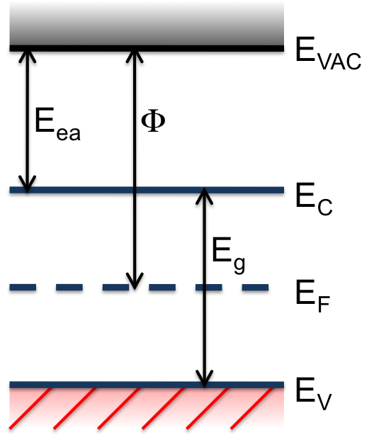
When an electron jumps to the conduction band, it leaves behind an empty spot in the valence band. This empty spot is called a hole, and it acts like a positive charge. Other nearby electrons in the valence band can move into this hole, making it seem as if the hole itself is moving. So, in a semiconductor, we have two types of charge carriers: negatively charged electrons in the conduction band and positively charged holes in the valence band.
Pure silicon doesn't conduct electricity very well on its own. To make it useful, we intentionally add tiny amounts of impurities in a process called doping. This allows us to control the number of available charge carriers.
doping
noun
The process of intentionally introducing impurities into a pure semiconductor to modify its electrical properties.
If we add an impurity that has an extra valence electron (like phosphorus), we create an excess of free electrons. This is called an n-type semiconductor, where 'n' stands for negative, the charge of the electron.
If we add an impurity that is missing a valence electron (like boron), we create an excess of holes. This is called a p-type semiconductor, where 'p' stands for positive, the effective charge of a hole.
The P-N Junction
Things get really interesting when we join a piece of p-type semiconductor with a piece of n-type semiconductor. This interface is called a p-n junction, and it's the fundamental building block for most semiconductor devices, including diodes, transistors, and solar cells.
As soon as the two materials touch, the excess electrons from the n-side start to diffuse over to the p-side to fill the abundant holes. Likewise, holes from the p-side diffuse to the n-side. This activity only happens in a very thin region right at the junction. As electrons leave the n-side, they leave behind positively charged atoms. When they fill holes on the p-side, they create negatively charged atoms. This creates a thin layer on either side of the junction that is depleted of free charge carriers, called the depletion region. This region has a built-in electric field that opposes any further diffusion of electrons and holes.
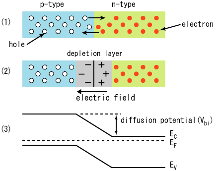
This setup creates a one-way street for electrical current. A p-n junction forms a device called a diode. By applying an external voltage, we can either shrink or widen the depletion region.
-
Forward Bias: If we connect the positive terminal of a battery to the p-side and the negative terminal to the n-side, we push the holes and electrons toward the junction. This shrinks the depletion region and allows current to flow easily.
-
Reverse Bias: If we flip the battery, we pull the charge carriers away from the junction. This widens the depletion region, blocking the flow of current.
This one-way-gate property is essential for converting alternating current (AC) to direct current (DC), a process called rectification.
Transistors The Digital Switch
While diodes are useful, the true revolution in electronics came with the invention of the transistor. A transistor is a semiconductor device with at least three terminals that can amplify an electrical signal or act as a switch.
By controlling a small current or voltage at one terminal, we can control a much larger current flowing through the other two. This is the principle behind both amplification (making a signal stronger) and switching (turning a current on or off). Billions of these microscopic switches working together are what allow computers to perform calculations.
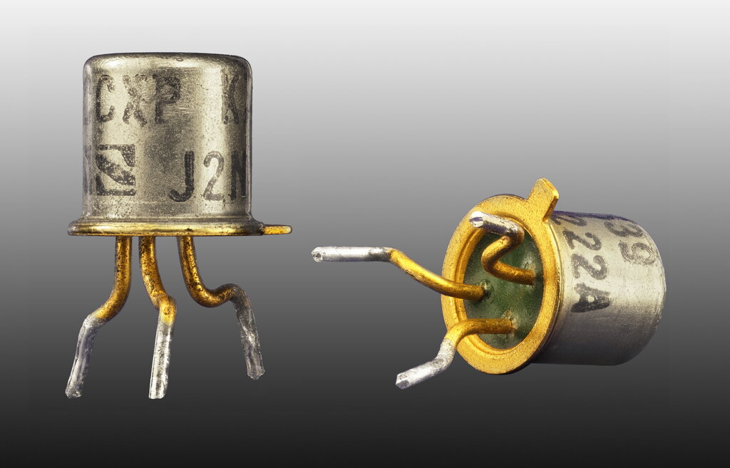
There are two main families of transistors: Bipolar Junction Transistors (BJTs) and Field-Effect Transistors (FETs).
Bipolar Junction Transistors (BJTs) consist of two p-n junctions sandwiched together, in either an N-P-N or P-N-P configuration. They have three terminals: the emitter, the base, and the collector. A small current flowing into the base terminal controls a much larger current flowing from the collector to the emitter. BJTs are current-controlled devices.
Field-Effect Transistors (FETs) also have three terminals: the source, the gate, and the drain. Unlike BJTs, FETs are voltage-controlled. A voltage applied to the gate creates an electric field that controls the flow of current through a channel between the source and the drain. No current flows into the gate itself, which makes FETs very efficient.
The most common type of FET is the MOSFET (Metal-Oxide-Semiconductor Field-Effect Transistor). MOSFETs are easier to miniaturize than BJTs and consume less power, making them the dominant type of transistor used in modern integrated circuits, like microprocessors and memory chips.
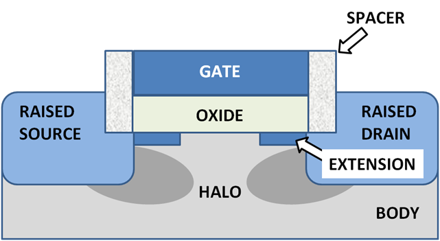
From the simple p-n junction in a diode to the billions of MOSFETs in a CPU, these semiconductor devices are the fundamental components that power our digital world. By controlling the flow of electrons and holes through carefully doped silicon, we can create the complex logic that underlies all of modern computation.
What is the defining characteristic of a semiconductor material?
In a semiconductor, for an electron to conduct electricity, it must jump from the valence band to the conduction band. What is the energy difference between these two bands called?