DIY RAM Module Engineering
Memory Cell Architecture
The Simplest Memory Circuit
How does a computer remember a single bit of information? It doesn't use magic, but a clever arrangement of logic gates called a latch. A latch is a circuit that has two stable states and can be used to store one bit (a 0 or a 1). The most fundamental type is the SR Latch, which stands for Set-Reset Latch.
An SR latch can be built from two cross-coupled NOR gates or two cross-coupled NAND gates. Let's look at the NOR gate version. The output of each NOR gate is fed back into one of the inputs of the other gate. This feedback loop is what allows the circuit to hold onto a value. The two other inputs, S (Set) and R (Reset), are used to control the state of the latch.
When you set S to 1 (and R is 0), the output Q becomes 1. This is the 'Set' state. If you then set S back to 0, the circuit 'remembers' the 1 because of the feedback loop. To change the output back to 0, you apply a 1 to the R input, which 'Resets' the latch. As long as both S and R are 0, the latch maintains its last state. A tricky situation arises if both S and R are 1 simultaneously; this leads to an undefined state where both outputs try to be 0, which violates the logic that Q and its inverse should be different. This is a key limitation of the basic SR latch.
| S | R | Q | Q' (Next State) |
|---|---|---|---|
| 0 | 0 | 0 | 0 (Hold) |
| 0 | 0 | 1 | 1 (Hold) |
| 0 | 1 | X | 0 (Reset) |
| 1 | 0 | X | 1 (Set) |
| 1 | 1 | X | ? (Invalid) |
Adding Control and Avoiding Problems
An SR latch reacts instantly to changes on its inputs. This isn't ideal for complex circuits where we need to coordinate actions precisely. To fix this, we can add a control input, often called an 'Enable' or '' signal. This creates a gated SR latch, where the Set and Reset inputs only have an effect when the Enable signal is active (e.g., high). This prevents the latch's state from changing at the wrong time.
While gating helps with timing, it doesn't solve the invalid S=1, R=1 state. A more robust solution is the D-type flip-flop. It simplifies the inputs to a single 'Data' (D) input and a clock input. Internally, it uses an SR latch but adds logic to ensure the invalid state can never happen. The D input is fed to S, and an inverted version of D is fed to R. This way, S and R are always opposites. When the clock signal pulses, the value at the D input is captured and stored, appearing at the Q output. This makes the D-type flip-flop a cornerstone of modern digital logic for capturing and holding data.
Sequential circuits use memory (e.g., flip-flops) to store and process data over time
Inside an SRAM Cell
On a silicon chip, logic gates are not discrete components but are built directly from transistors. The most common design for a single bit of Static RAM () is the 6T cell, meaning it uses six transistors. This design is essentially two cross-coupled inverters forming a latch, plus two additional 'access' transistors.
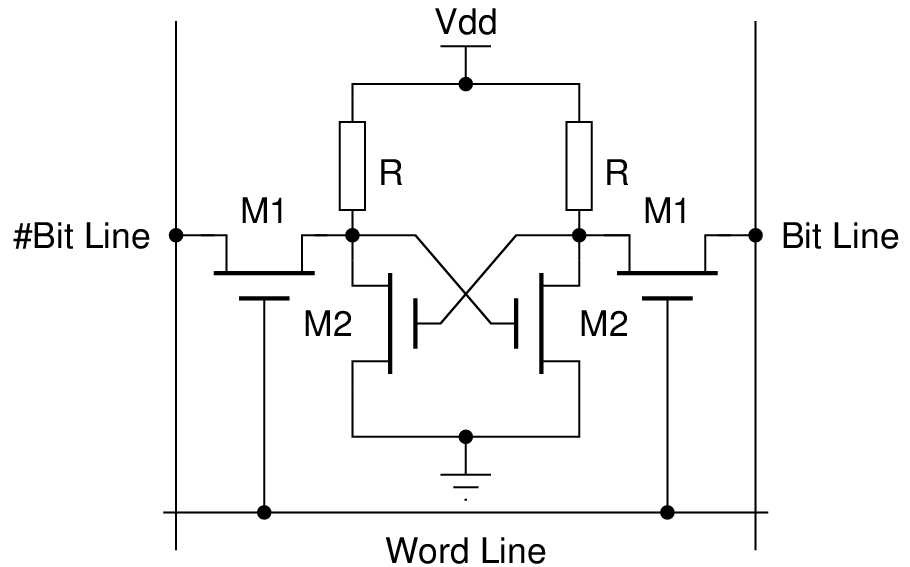
The core of the cell consists of four transistors (M1 through M4 in many diagrams) arranged as two inverters pointing at each other. This is the latch that stores the bit. If one inverter's output is 1, it forces the other inverter's output to 0, which in turn holds the first inverter's output at 1. The state is stable.
The other two transistors act as switches. They are controlled by the 'Word Line'. When the Word Line is activated, these switches close, connecting the internal latch to the 'Bit Line' and '#Bit Line'. This allows the system to either read the state of the latch or write a new state into it by overpowering the current state of the inverters.
This 6T architecture provides a fast and reliable way to store a single bit of data. By combining millions or billions of these cells into an array, we build the fast cache memory that is essential for modern processor performance.