Digital Logic Design Fundamentals
Advanced Combinational Logic
Data Routers and Selectors
Beyond basic AND and OR gates, combinational logic circuits use larger building blocks to manage data flow efficiently. Think of these components as the traffic controllers of the digital world. The most fundamental of these are multiplexers and demultiplexers.
Multiplexer
noun
A device that selects one of several analog or digital input signals and forwards it into a single output line. A multiplexer of 2^n inputs has n select lines.
A multiplexer, or MUX, is a digital switch. It has multiple data inputs, a few selection lines, and just one output. The selection lines act as a binary address, telling the MUX which specific input to pass through to the output. For instance, a 4-to-1 MUX uses two selection lines (, ) to choose one of four inputs ( through ). If the selection lines are set to binary 10 (decimal 2), then input is routed to the output.
A demultiplexer (DEMUX) does the exact opposite. It takes a single input and distributes it to one of many outputs. Again, selection lines determine which output path is chosen. This is invaluable for tasks like in memory systems, where a processor needs to select a specific memory chip out of many on a shared data bus.
Shorthand and Longhand
Encoders and decoders are another pair of complementary components that help manage information. An encoder converts a set of signals into a more compressed code, while a decoder expands that code back into its original form.
A common example is a priority encoder, which takes multiple input lines and outputs the binary representation of the highest-priority active input. For example, in an 8-to-3 encoder, if input lines 2 and 5 are both active, and line 5 has higher priority, the output will be binary 101 (decimal 5).
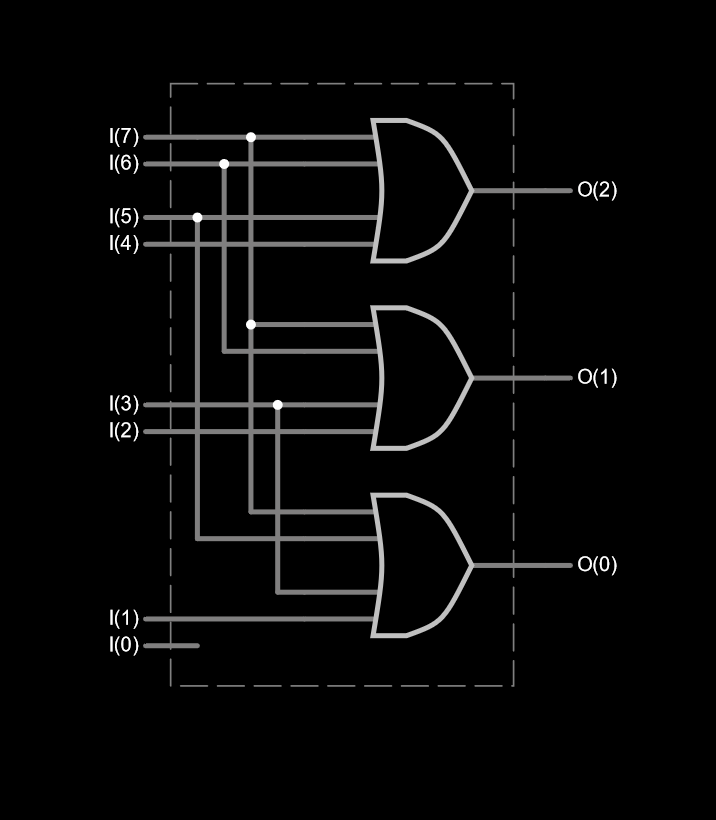
Decoders are used everywhere, from turning on the right segments in a 7-segment display to selecting which device to enable on a computer bus. A 3-to-8 decoder, for instance, takes a 3-bit binary input and activates one of eight corresponding output lines. An input of '011' would activate only the third output line.
Physical Implementation
Knowing the logical function is only half the battle. How these circuits are physically built impacts their performance. Two dominant logic families have been and CMOS.
-
TTL (Transistor-Transistor Logic): An older family based on bipolar junction transistors. It's known for being fast and robust, but it consumes a significant amount of power, even when idle.
-
CMOS (Complementary Metal-Oxide-Semiconductor): The modern standard, using pairs of complementary MOSFETs. Its primary advantage is extremely low static power consumption. It only draws significant current when the transistors are switching states. However, it can be more susceptible to damage from electrostatic discharge.
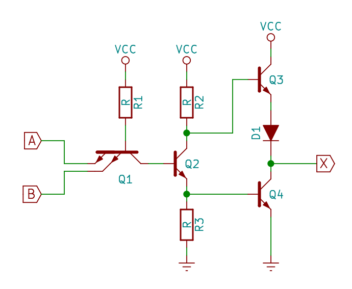
These physical differences lead to important trade-offs. While CMOS is the clear winner for battery-powered devices, TTL's speed and drive capability made it a long-time favorite for high-speed systems where power was less of a concern. Modern logic often integrates the best of both worlds, using BiCMOS technology.
| Characteristic | TTL (Transistor-Transistor Logic) | CMOS (Complementary MOS) |
|---|---|---|
| Static Power | High | Very Low |
| Switching Speed | Fast | Can be slower, but modern versions are very fast |
| Noise Margin | Good | Excellent |
| Input Impedance | Low | High (susceptible to static) |
| Voltage Levels | Strict (e.g., 0V-0.8V for LOW) | Flexible (wider range) |
Timing and Hazards
In the real world, signals don't change instantly. The time it takes for a gate's output to respond to a change in its input is called propagation delay (). While measured in nanoseconds, these tiny delays add up in complex circuits.
When different signal paths to a single gate have different total propagation delays, a problem called a hazard can occur. This creates a brief, unwanted glitch on the output as the inputs arrive at slightly different times.
For example, in the expression $Y = A · B + eg A · C$, if B and C are both 1, the output Y should always be 1 regardless of A's value. However, when A switches from 1 to 0, the first term ($A · B$) becomes 0 slightly before the second term ($ eg A · C$) becomes 1 due to the delay of the NOT gate. This causes Y to briefly drop to 0. These hazards can be eliminated by adding redundant logic terms that cover these transitional gaps.
Building circuits with these higher-level MSI components like multiplexers and decoders, rather than just individual gates, is a key design strategy. It simplifies the design process, often reduces chip count, and can help manage timing issues by using pre-characterized, optimized building blocks.
How many selection lines are required for a 16-to-1 multiplexer?
What is the primary functional difference between a multiplexer (MUX) and a demultiplexer (DEMUX)?