Demystifying Computer Memory Architecture
Memory Bus Architecture
The Data Highway
The CPU and RAM are in constant communication, but they don't talk directly. They need a mediator to manage the flow of data. For years, this job belonged to a dedicated chip on the motherboard called the Northbridge, or Memory Controller Hub (MCH). It acted as a traffic cop, sitting between the CPU, RAM, and other high-speed components like the graphics card.
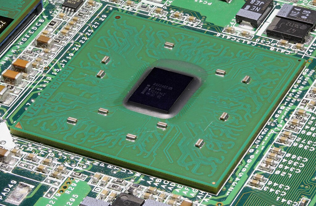
This setup worked, but having a separate chip introduced a slight delay, a bottleneck. As CPUs got faster, this delay became more noticeable. The solution was to move the memory controller directly onto the CPU die itself. This is the standard today, known as an integrated memory controller (IMC). By putting the controller on the same piece of silicon as the processor, the physical distance data has to travel is dramatically reduced, cutting down latency and speeding everything up.
The Three Lanes of Traffic
Regardless of whether the controller is on the motherboard or in the CPU, it uses a system of electrical pathways called a bus to communicate with RAM. Think of it as a highway system with three distinct parts, each with a specific job.
This system ensures that data gets to the right place, at the right time, and that the CPU and RAM know what to do with it. Each bus is a collection of tiny wires, or traces, on the motherboard.
| Bus Type | Direction | Purpose |
|---|---|---|
| Address Bus | Unidirectional (CPU to RAM) | Specifies the memory address. It's like the postal address on a letter; it tells memory where to look. |
| Data Bus | Bidirectional | Carries the actual data. This is the letter inside the envelope, going to or from the specified address. |
| Control Bus | Bidirectional | Transmits timing and command signals. It tells RAM whether to perform a read or a write operation and coordinates the action. |
Speed and Bandwidth
The performance of this memory highway is determined by two key factors: its width and its speed.
The bus width, measured in bits, refers to the number of parallel wires in the data bus. A 64-bit data bus can transfer 64 bits (or 8 bytes) of data simultaneously. Modern consumer systems almost universally use a 64-bit wide bus for each memory channel.
The bus speed, or frequency, is measured in Megahertz (MHz). It dictates how many times per second data can be sent across the bus. Modern RAM is often labeled with its data rate in megatransfers per second (MT/s), which is typically double its clock frequency thanks to a technique called Double Data Rate (DDR).
For example, a system with a single channel of DDR5-5200 RAM has a bus clock of 2600 MHz and a data bus width of 64 bits (8 bytes). The maximum theoretical bandwidth would be MB/s, or 41.6 GB/s.
Maintaining signal integrity is a major engineering challenge. At such high frequencies, the electrical signals traveling down these tiny copper traces can be affected by interference from neighboring traces (crosstalk) or reflections from the end of the line. Motherboard designers must carefully route these traces, control their impedance, and use proper termination to ensure the data arrives clean and uncorrupted. These physical and electrical constraints are often the limiting factor in how fast memory can run.
What was the name of the dedicated chip on the motherboard that historically managed the flow of data between the CPU and RAM?
What is the primary advantage of moving the memory controller from the motherboard (as a Northbridge) to the CPU die (as an IMC)?
Understanding this data highway is key to seeing how hardware specs translate into real-world performance.