CMOS Integrated Circuit Layout
CMOS Basics
The Two Sides of the Switch
Nearly every digital device you own is powered by a technology called CMOS, which stands for Complementary Metal-Oxide-Semiconductor. It’s the standard way we build integrated circuits, or chips. The “complementary” part is the key idea. CMOS technology uses two different types of transistors that work together like a perfectly coordinated team.
Think of a transistor as a tiny, electrically controlled switch. In CMOS, we have two kinds: NMOS and PMOS. They are designed to be opposites. When one is on, the other is off. This simple pairing is what makes modern electronics so powerful and efficient.
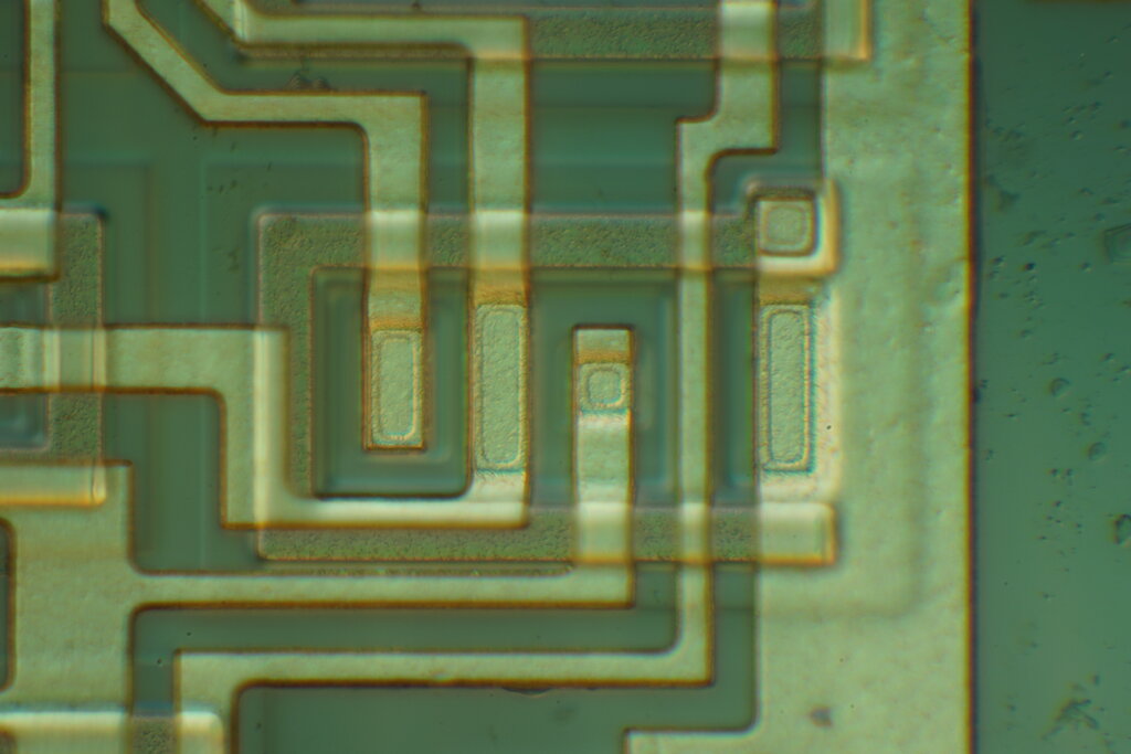
Meet the Transistors
Let's break down the two types of transistors that form the foundation of CMOS circuits.
An NMOS (n-channel MOS) transistor turns ON when its gate receives a high voltage (a logic '1'). A PMOS (p-channel MOS) transistor does the opposite, turning ON when its gate receives a low voltage (a logic '0').
An NMOS transistor is built on a slice of silicon doped to be p-type (meaning it has an excess of positive charge carriers). It has two n-type regions called the source and drain. Above the channel between them is a thin insulating layer and a gate. Applying a positive voltage to the gate attracts electrons, creating a conductive n-channel that allows current to flow. Because it connects a circuit's output to ground, it's known as a pull-down transistor.
A PMOS transistor is its mirror image. It's built on an n-type substrate with p-type source and drain regions. Applying a low or zero voltage to the gate allows positive charge carriers (called holes) to form a p-channel, enabling current flow. Since it connects the output to the power supply, it's called a pull-up transistor.
A Perfect Pair
The magic of CMOS happens when we combine these two opposing transistors. The most basic CMOS circuit is an inverter, which flips a logic signal from 1 to 0 or 0 to 1. In an inverter, a PMOS transistor is connected to the power supply (), and an NMOS transistor is connected to ground. Their gates are tied together to form the input, and their drains are tied together to form the output.
When the input is high (1), the NMOS turns on and the PMOS turns off. The output is pulled down to ground, becoming low (0). When the input is low (0), the PMOS turns on and the NMOS turns off. The output is pulled up to the power supply, becoming high (1).
This design has a huge advantage: in a steady state (either high or low), one of the transistors is always off. This means there's no direct path from power to ground, and the circuit consumes almost no power. Power is only drawn during the brief moment of switching.
This low static power consumption is the primary reason CMOS technology dominates the industry, especially for battery-powered devices. It also offers high immunity to electrical noise and can operate at high speeds, making it ideal for everything from microprocessors to memory chips.
Building a Chip
Creating these tiny structures is an incredibly complex process called fabrication, which takes place in highly controlled environments called cleanrooms. It starts with a pure silicon wafer.
Through a series of steps involving high temperatures, chemical deposition, and light-based patterning (photolithography), layers of different materials are added and etched away. This process, repeated dozens of times, builds up the NMOS and PMOS transistors and the metal wires that connect them, eventually forming a complete integrated circuit.
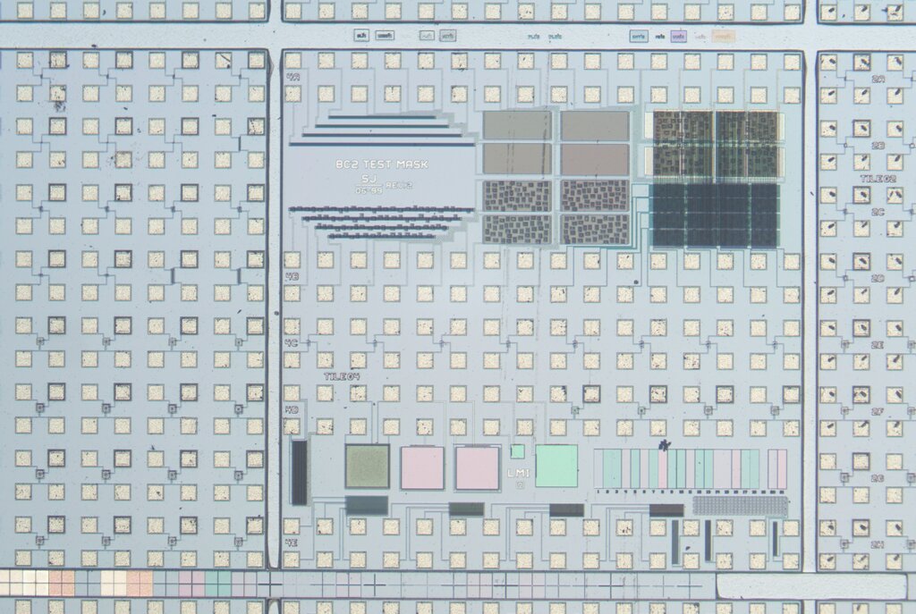
While the details are intricate, the core goal is to precisely create millions or billions of these complementary NMOS and PMOS pairs according to a designer's blueprint. The result is a powerful, efficient chip that forms the brain of our electronic world.
Let's check your understanding of these core concepts.
What does the "C" in CMOS stand for?
In a standard CMOS inverter, what is the state of the transistors when the input is LOW (logic 0)?