Applied RF Engineering
RF Component Practicalities
Beyond the Ideal Circuit
In the world of schematics, transmission lines are perfect conductors and components behave exactly as their symbols suggest. But when you move from paper to a physical circuit board, reality sets in. At radio frequencies, the neat rules of ideal circuits bend. Seemingly simple copper traces and passive components reveal complex personalities, introducing losses, delays, and reflections that can derail a design.
These real-world effects aren't just minor annoyances; they are fundamental challenges in RF engineering. A signal traveling down a microstrip line on a PCB loses energy due to resistance in the copper and imperfections in the dielectric material separating it from the ground plane. This isn't just a simple power drop. Different frequency components of a signal can travel at slightly different speeds, a phenomenon called dispersion, which distorts the signal's shape.
Furthermore, at high frequencies, current doesn't use the entire conductor. It crowds near the surface, a behavior known as the This effectively shrinks the conductor's cross-sectional area, increasing its resistance. If another current-carrying conductor is nearby, the currents will redistribute to either crowd together or push apart, which is called the proximity effect. Both of these phenomena are frequency-dependent, meaning resistance increases as frequency goes up, adding another layer of complexity to high-speed design.
The Art of Impedance Matching
You already know that mismatched impedances cause reflections, leading to power loss and signal distortion. In the real world, achieving a perfect match requires specialized networks. The goal is always the same: make the load impedance look like the source's characteristic impedance (usually 50 Ω) to ensure maximum power transfer.
For this, engineers use impedance matching networks. Simple networks can be built from discrete inductors and capacitors, known as lumped elements. The most common are L-networks, which use one series and one shunt component. For more complex matching problems, T-networks or Pi-networks offer more flexibility.
At very high frequencies, the parasitic effects of these lumped components can become a problem. An alternative is to use distributed elements, which are essentially carefully shaped sections of transmission line. A common example is a stub tuner, where a short section of transmission line is connected in parallel or series with the main line. By controlling the stub's length and position, you can cancel out the reactive part of the load impedance. Another critical component is a balun (balanced to unbalanced), which is used to connect balanced antennas, like a dipole, to unbalanced transmission lines, like coaxial cable, while also performing an impedance transformation.
Choosing the right physical connectors and cables is just as important as designing the circuit itself. Each has trade-offs in terms of cost, size, frequency range, power handling, and durability. For lab work and internal connections, SMA connectors are common. For high-power applications or outdoor equipment, the larger, more robust N-type connector is often preferred.
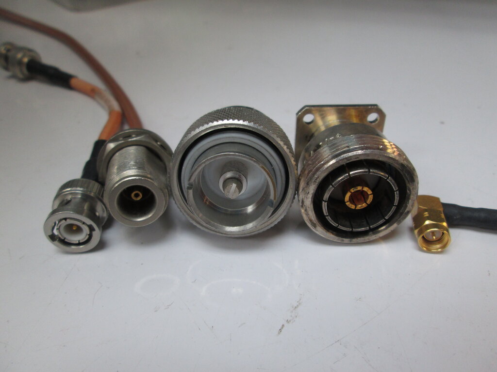
When selecting a cable, you must consider its loss (specified in dB per meter at a given frequency), its power handling capability, and its Voltage Standing Wave Ratio (VSWR), which is another measure of impedance match. A low VSWR is desirable. Mechanical properties, like flexibility and minimum bend radius, are also critical, especially in systems where components might move or vibrate.
When Components Misbehave
At radio frequencies, a resistor is never just a resistor. It also has a small amount of series inductance from its leads and body, and parallel capacitance between its end caps. Similarly, an inductor has parasitic capacitance between its windings, and a capacitor has parasitic series inductance (ESL) and resistance (ESR). These aren't design flaws; they're unavoidable consequences of physics.
These parasitics create a (SRF) for every component. Below its SRF, an inductor acts like an inductor, and a capacitor acts like a capacitor. But at its SRF, the component's inductive and capacitive reactances cancel out, and it behaves like a pure resistor. Above its SRF, the component's behavior flips: an inductor starts acting like a capacitor, and a capacitor acts like an inductor. This is why component datasheets for RF applications always specify the SRF. A 10 nF capacitor might be perfect for filtering at 1 MHz, but it could behave like an inductor at 1 GHz, making the circuit fail completely.
Understanding these non-ideal behaviors is crucial when using S-parameters to characterize components. The S-parameters you measure for a real capacitor will clearly show its transition from capacitive to inductive behavior as the frequency crosses its SRF. This is why simulating a design with accurate, frequency-dependent models for every component, connector, and PCB trace is a standard step in modern RF design. Even the physical placement of components on a board matters, as nearby traces can capacitively or inductively couple to each other, creating unintended signal paths.
Ready to test your knowledge of these real-world RF effects?
What is the primary consequence of the skin effect in a conductor at high radio frequencies?
A capacitor is used in a filter circuit designed to operate at 5 GHz. However, the chosen capacitor has a Self-Resonant Frequency (SRF) of 2 GHz. How will this component behave in the circuit at its 5 GHz operating frequency?
Moving from ideal models to real-world components introduces a new set of rules. By understanding and accounting for these practicalities, you can design RF systems that are robust and perform as intended.