Advanced PCB Design with KiCad
Advanced Routing Techniques
Routing Differential Pairs
When you're working with high-speed signals like USB or Ethernet, you can't just run single wires. These signals travel in pairs, called differential pairs. One wire carries the signal, and the other carries an identical, inverted version.
The magic of this setup is noise cancellation. Any external electromagnetic interference (EMI) that hits the wires will affect both of them almost identically. A differential receiver at the end looks only at the difference between the two signals. Since the noise added the same voltage to both, it gets subtracted out and ignored. This makes the signal much more robust against noise.
To route these in KiCad, you first define them in the schematic. Name the nets with a + and - suffix, like USB_D+ and USB_D-. KiCad will automatically recognize them as a pair.
In the PCB editor, use the "Route Differential Pairs" tool. Click on one of the pads, and KiCad will route both traces simultaneously, keeping them parallel and at a specific distance. Your main job is to guide them to their destination. The key is to keep the traces as close to the same length as possible and avoid sharp turns.
Length Matching Traces
Imagine a bus carrying data from a memory chip to a processor. If all the bits of a single byte don't arrive at the exact same time, the processor will read garbage. Even a tiny delay, or skew, caused by one trace being a few millimeters longer than another can corrupt the data at high speeds.
Length matching is the process of ensuring that a group of related traces, like a data bus, have identical lengths. This guarantees that all signals arrive at their destination simultaneously.
For high-speed signals, arriving a nanosecond too late is the same as not arriving at all.
KiCad has a dedicated tool for this. First, route all the traces in the bus. Then, use the "Tune Skew / Phase" tool (often called the length tuning tool). You select the longest trace in the group as your reference. Then, you click on each of the shorter traces.
As you move your mouse, KiCad will add serpentine sections, often called trombones, to the trace. This increases its length without changing its start or end point. A small dialog shows you the target length and the current length, so you can add bumps until the lengths match perfectly.
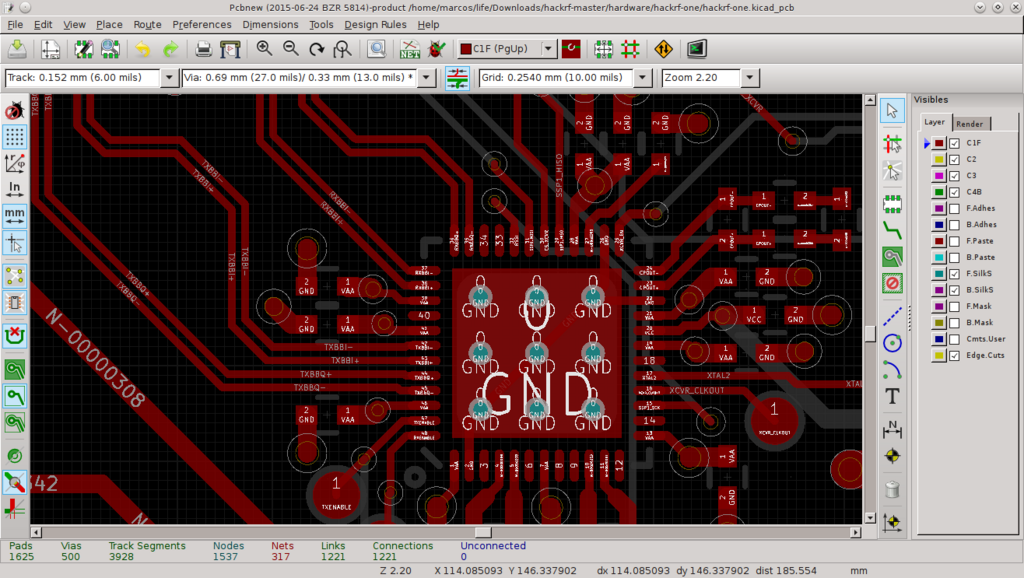
Controlling Impedance
At high frequencies, a PCB trace doesn't just act like a simple wire; it acts like a transmission line. Every transmission line has a characteristic impedance, which is a measure of how much it resists the flow of alternating current. For signals to transfer cleanly from a source chip to a destination chip, the impedance of the trace must match the impedance of the chips (commonly 50 ohms for single-ended signals or 90-100 ohms for differential pairs).
If the impedances don't match, signal reflections occur. Part of the signal's energy bounces back from the destination, distorting the original signal. This can cause errors and system failure.
When routing on a PCB you want to minimize the length of each trace as much as possible.
Controlling impedance involves carefully calculating the right trace width for a given PCB stackup. The impedance depends on:
- The width of the copper trace.
- The thickness of the copper.
- The distance to a reference plane (usually a ground or power plane).
- The dielectric constant of the PCB material (like FR-4).
KiCad has a built-in calculator (PCB Calculator -> TransLine) to help you determine the correct trace width. You input your PCB manufacturer's stackup details, and it tells you what width to use for your desired impedance. Once you know the width, you set up a custom design rule in File -> Board Setup -> Net Classes. You can create a new net class called 50-ohm for example, set the trace width there, and assign all your high-speed signals to that class.
What is the primary advantage of using differential pairs for high-speed signals?
In KiCad, how do you typically define two nets in the schematic to be recognized as a differential pair in the PCB editor?
Mastering these techniques is essential for any modern PCB design. They ensure your high-speed circuits are reliable and perform as expected.