ADS1299 Firmware Timing and Integrity Analysis
ADS1299 Timing Foundations
The Clock's Cadence
The master clock, or , is the heartbeat of the ADS1299. It drives the internal modulator and dictates the pace of every analog-to-digital conversion. This clock signal isn't just a simple pulse; it's the fundamental reference against which all timing is measured. The stability and precision of directly impact the quality and timing of your data.
The relationship between the master clock and the final output data rate, , is governed by the Oversampling Ratio (OSR). The ADS1299 uses oversampling to improve resolution and reduce noise. You control this ratio through the DR[2:0] bits in the CONFIG1 register, effectively telling the device how many internal samples to average for each data point it outputs.
For a standard of 2.048 MHz, selecting a data rate of 250 SPS in the register sets an OSR of 8192. This means the device is performing 8192 internal modulator cycles for every single data sample that is sent to your microcontroller. This process is crucial for achieving the high-resolution, low-noise performance required for biopotential measurements.
| Data Rate (SPS) | CONFIG1 DR[2:0] | Oversampling Ratio (OSR) |
|---|---|---|
| 16,000 | 000 | 128 |
| 8,000 | 001 | 256 |
| 4,000 | 010 | 512 |
| 2,000 | 011 | 1024 |
| 1,000 | 100 | 2048 |
| 500 | 101 | 4096 |
| 250 | 110 | 8192 |
From Rate to Interval
Knowing the data rate allows us to calculate the theoretical time between consecutive data samples, the frame interval, which we'll call . This value is simply the inverse of the data rate. It represents the ideal, perfectly consistent duration between each data packet your firmware should expect.
Using our 250 SPS example, the expected interval is $1 / 250$ Hz, which equals 4 milliseconds. This calculation forms the baseline for validating the timing of your data acquisition system. When you analyze firmware logs, the timestamps of incoming packets should cluster tightly around this 4 ms interval.
The DRDY Signal
The ADS1299 doesn't just send data whenever it feels like it. It signals the microcontroller when a new conversion is complete and the data is ready to be read. This is the job of the DRDY signal, an active-low output pin. When DRDY transitions from high to low, it acts as an interrupt, telling your processor, "I have a new sample for you. Come and get it."
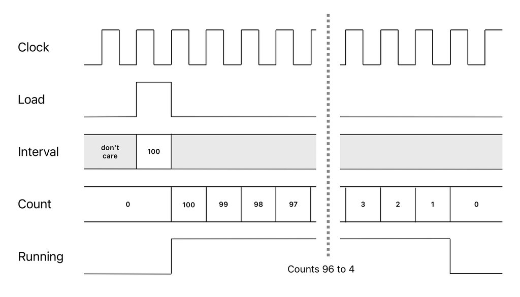
The timing of this signal is predictable. A new conversion begins on the 4th falling edge of after the previous DRDY pulse goes high. The conversion itself takes a specific number of clock cycles, defined by the OSR. The next DRDY pulse will go low precisely clock cycles after the conversion started. This predictable rhythm is the foundation of a stable data acquisition pipeline.
Clock Jitter and Its Effects
In an ideal world, the master clock would be perfectly stable. In reality, all clock sources have some amount of —small, random variations in the timing of the clock edges. This isn't just an academic concern; clock jitter directly affects the precision of the ADC.
The sampling instant is defined by the clock edge. If the edge's timing varies, the voltage being measured might be slightly different, introducing an error into the conversion.
The ADS1299 is sensitive to jitter on the input. For this reason, using a high-quality, low-jitter crystal oscillator is essential for achieving the performance levels specified in the datasheet. A noisy clock source generated by a microcontroller's internal PLL, for example, could compromise the integrity of your measurements by introducing timing uncertainty into the very heart of the conversion process.
What is the primary function of the master clock, , in the ADS1299?
If the ADS1299 is configured for a data rate () of 500 SPS (Samples Per Second), what is the expected time interval () between consecutive data samples?