VLSI Systems and Design
CMOS Fabrication Fundamentals
From Logic to Layout
You know that digital circuits are built from logic gates like AND, OR, and NOT. But how do these abstract ideas become a physical object? A schematic diagram is a blueprint, but manufacturing a chip involves turning that blueprint into a complex, three-dimensional structure on a slice of silicon. This transformation from logic to layout is the heart of Very Large-Scale Integration (VLSI) design.
The dominant technology for this process is CMOS, or Complementary Metal-Oxide-Semiconductor. It uses pairs of two different types of transistors, NMOS and PMOS, to create efficient, low-power logic gates. Let's walk through how these microscopic switches are built from the ground up.
The N-Well Fabrication Process
Everything starts with a silicon wafer, a thin, circular disc of highly pure, crystalline silicon. For a typical CMOS process, we begin with a wafer that is lightly doped to be a p-type semiconductor. This forms the base, or substrate, for all the components. The goal is to build both NMOS and PMOS transistors on this single substrate. NMOS transistors can be built directly on the p-type substrate, but PMOS transistors require an n-type environment.
To solve this, we create localized n-type regions called for the PMOS transistors. This is the first major step in what's known as the n-well process. This process involves a sequence of adding and removing materials in precise patterns, a technique called which acts like a sophisticated stenciling system. Using a series of masks, we expose specific parts of the wafer to light, which allows us to selectively etch away materials or implant new atoms to change the properties of the silicon.
After creating the n-wells, a very thin, high-quality layer of silicon dioxide (SiO₂) is grown across the wafer. This will serve as the gate insulator, a crucial component that prevents the gate from shorting to the silicon underneath. Next, a layer of polysilicon is deposited. This layer will be patterned using another photolithography step to form the gates for all the transistors. The gate is the 'switch' that controls whether the transistor is on or off.
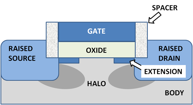
With the gates in place, we create the source and drain regions. This is done through a process called ion implantation, where the wafer is bombarded with ions to create n-type and p-type regions. A mask ensures that only the correct areas are doped. The polysilicon gates handily act as a self-aligning mask, preventing the area directly beneath them from being doped. This creates n+ regions for the NMOS source/drain and p+ regions for the PMOS source/drain.
Finally, the whole structure needs to be wired together. A thick insulating layer of oxide is deposited over everything. Another photolithography and etching step is used to open contact holes where connections are needed. Then, a layer of metal (typically copper or aluminum) is deposited, filling these holes and creating the interconnects that link the gates, sources, and drains to form the complete circuit. For complex chips, this metallization process can be repeated multiple times to create a dense web of wiring.
The Rules of the Road
You can't just draw transistors of any size or place them arbitrarily close to each other. The fabrication process has physical limitations. To ensure a design can be manufactured reliably, engineers must follow a set of geometric constraints known as These rules are specific to each fabrication technology, often identified by the minimum feature size, like the 7nm or 5nm node.
These rules define the minimum width of a metal line, the minimum spacing between two lines, the required overlap between layers, and hundreds of other constraints. Adhering to them guarantees that, despite minor imperfections in the manufacturing process, the final chip will function as intended. Software tools automatically perform a Design Rule Check (DRC) to find and flag any violations before the design is sent for fabrication, saving millions of dollars in wasted manufacturing runs.
| Rule Type | Description | Why it Matters |
|---|---|---|
| Width | The minimum allowed width of any shape on a layer. | A wire that's too thin might break or carry insufficient current. |
| Spacing | The minimum distance between two shapes on the same layer. | Features that are too close might accidentally merge, causing a short circuit. |
| Overlap | The minimum amount one layer must overlap another. | Ensures a reliable electrical connection, for instance between a metal contact and the silicon below. |
| Enclosure | How much one layer must surround another. | A contact cut needs to be fully enclosed by the metal layer above it to ensure a good connection. |
Layout of a CMOS Inverter
Let's apply these concepts to the simplest CMOS gate: the inverter. An inverter consists of one PMOS and one NMOS transistor. The layout translates the schematic into a physical floorplan.
In the layout, you can see the layers we discussed. The PMOS transistor is the region where the polysilicon gate crosses over the p+ diffusion area inside the n-well. The NMOS transistor is where the same polysilicon gate crosses the n+ diffusion on the p-substrate. Metal layers provide power (VDD and VSS/Ground) and connect the drains of both transistors to form the output. Each feature's size and spacing strictly follows the design rules for that technology.
What is the primary purpose of an n-well in a CMOS process that uses a p-type substrate?
The process used to transfer a circuit pattern onto a silicon wafer using masks and light is called ______.
Understanding this fabrication sequence is the first step in appreciating how a logical design becomes a functioning piece of silicon. Every choice in a chip's layout is a trade-off between performance, power, area, and the strict realities of manufacturing.