Semiconductor Supply Chain Risks
Semiconductor Supply Chain Overview
The Journey of a Chip
Every microchip starts its life as something surprisingly common: sand. Specifically, the silicon dioxide in sand is the raw material for nearly all semiconductors. This sand is purified into electronic-grade silicon, a material that is 99.9999999% pure. This ultra-pure silicon is then melted and grown into large, cylindrical crystals called ingots.
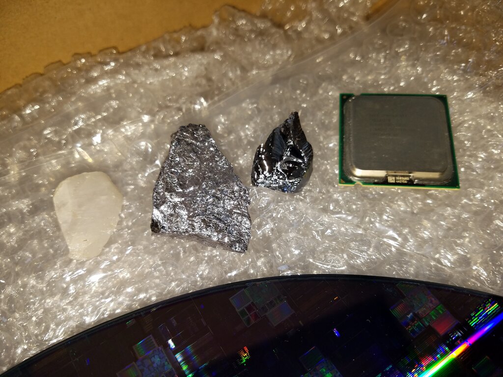
These ingots, which can weigh over 100 kilograms, are sliced into incredibly thin discs known as wafers. A typical wafer is about the thickness of a credit card but much larger in diameter, often 300 millimeters (about 12 inches). This polished, pristine wafer is the canvas on which hundreds or even thousands of identical chips will be created.
Inside the Fab
The magic of turning a blank wafer into a complex grid of microchips happens inside a semiconductor fabrication plant, or "fab." These are some of the cleanest places on Earth, as even a single speck of dust can ruin a chip. The process involves hundreds of steps, but it all begins with design.
Chip architects use specialized Electronic Design Automation (EDA) software to create intricate, multi-layered blueprints for the chip's circuitry. This design is then transferred onto the silicon wafer in a process called photolithography. It works a bit like developing a photograph. A light-sensitive material is spread over the wafer, and a pattern, or mask, is placed over it. When exposed to ultraviolet (UV) light, the pattern of the mask is etched onto the wafer. This process is repeated dozens of times, building the chip layer by layer.
Between lithography steps, other processes like deposition (adding thin layers of material), etching (removing material), and doping (introducing impurities to change silicon's electrical properties) take place. Together, these steps build up the transistors, wires, and other components that form the integrated circuit. The features created can be incredibly small, measured in nanometers—billionths of a meter.
Packaging and Testing
Once all the layers are complete, the wafer is a mosaic of finished chips, still connected as one piece. The next stage is Assembly, Test, and Packaging (ATP). The wafer is sliced with a diamond saw to separate the individual chips, which are called dies.
Each tiny die is then tested to see if it works correctly. Functional dies are moved to the next step: assembly. The die is mounted onto a substrate, and microscopic wires are bonded to connect it to the external pins you see on a finished chip. Finally, the entire assembly is enclosed in a protective plastic or ceramic casing. This is the familiar black rectangle we recognize as a computer chip.
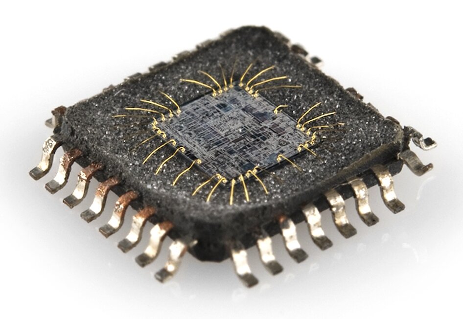
After packaging, the chips go through a final round of testing to ensure they weren't damaged during assembly and can perform under real-world conditions, like high temperatures. Only the chips that pass this rigorous quality control are shipped to customers.
A Global Production Line
The semiconductor supply chain is not contained within one factory or even one country. It is a highly specialized and globally distributed network. Different stages are often handled by different companies in different parts of the world.
-
Design and EDA: The intellectual heavy lifting of chip design, along with the creation of the essential EDA software, is concentrated in the United States.
-
Manufacturing Equipment: The complex machinery needed for fabrication comes from a few key countries. The most advanced lithography machines, for instance, are made exclusively by a single company in the Netherlands.
-
Wafer Fabrication: The most capital-intensive stage, manufacturing the wafers, is dominated by foundries in Taiwan and South Korea.
-
Assembly, Test, and Packaging (ATP): The final stages are more labor-intensive and are largely concentrated in Southeast Asian countries like Malaysia, Vietnam, and the Philippines, as well as in China.
A single chip can travel thousands of miles and cross international borders multiple times before it's installed in a device.
This intricate global dance of design, fabrication, and assembly allows for incredible efficiency and specialization. Each region contributes a critical piece of the puzzle, coming together to produce the chips that power our world.
Let's review the key stages and terms we've covered.
What is the primary raw material used to create the ultra-pure silicon for microchips?
In a semiconductor fab, what is the process of using UV light to etch a chip's design onto a silicon wafer called?
This complex, globe-spanning process ensures that the building blocks of modern technology are constantly being produced, from raw sand to the finished product in your hands.